ATA121302 데이터 시트보기 (PDF) - ANADIGICS
부품명
상세내역
제조사
ATA121302 Datasheet PDF : 8 Pages
| |||
ATA121302
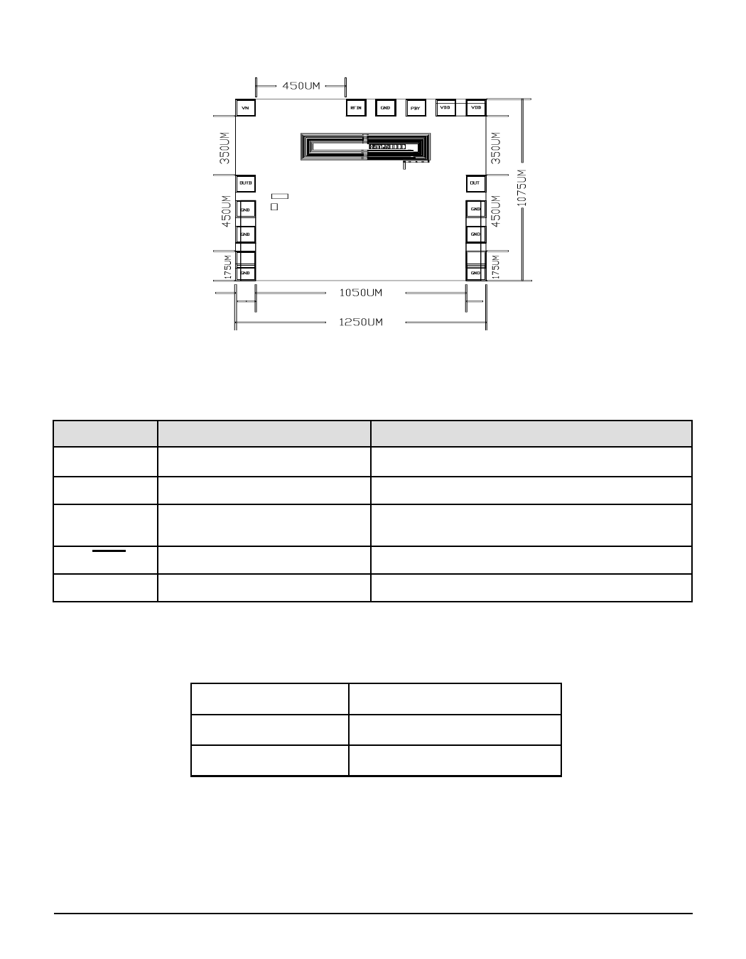
Figure 2: Bonding Pad Layout
PAD
VDD
IIN
VN
VOUT
VOUT
Table 1: ATA121302 Pad Description
DESCRIPTION
COMMENT
Positive Supply Voltage
+ 5 Volts
TIA Input
Connect to detector cathode for proper operation
Negative Voltage for Photodiode
Biasing
Connect to detector anode for optimum performance
TIA Output Voltage (Non-Inverted) Logical '1' with optical input
TIA Output Voltage (Inverted)
Logical '0' with optical input
ELECTRICAL CHARACTERISTICS
Table 2: Absolute Maximum Ratings
VDD
7.0V
II N
3.5mA
TS
Storage Temp. -65 0C to 125 0C
Stresses in excess of the absolute ratings may cause
permanent damage. Functional operation is not implied under
these conditions. Exposure to absolute ratings for extended
periods of time may adversely affect reliability.
2
ADVANCED PRODUCT INFORMATION - Rev 0.1
08/2001
Share Link: 