ATA6602(2009) 데이터 시트보기 (PDF) - Atmel Corporation
부품명
상세내역
제조사
ATA6602 Datasheet PDF : 361 Pages
| |||
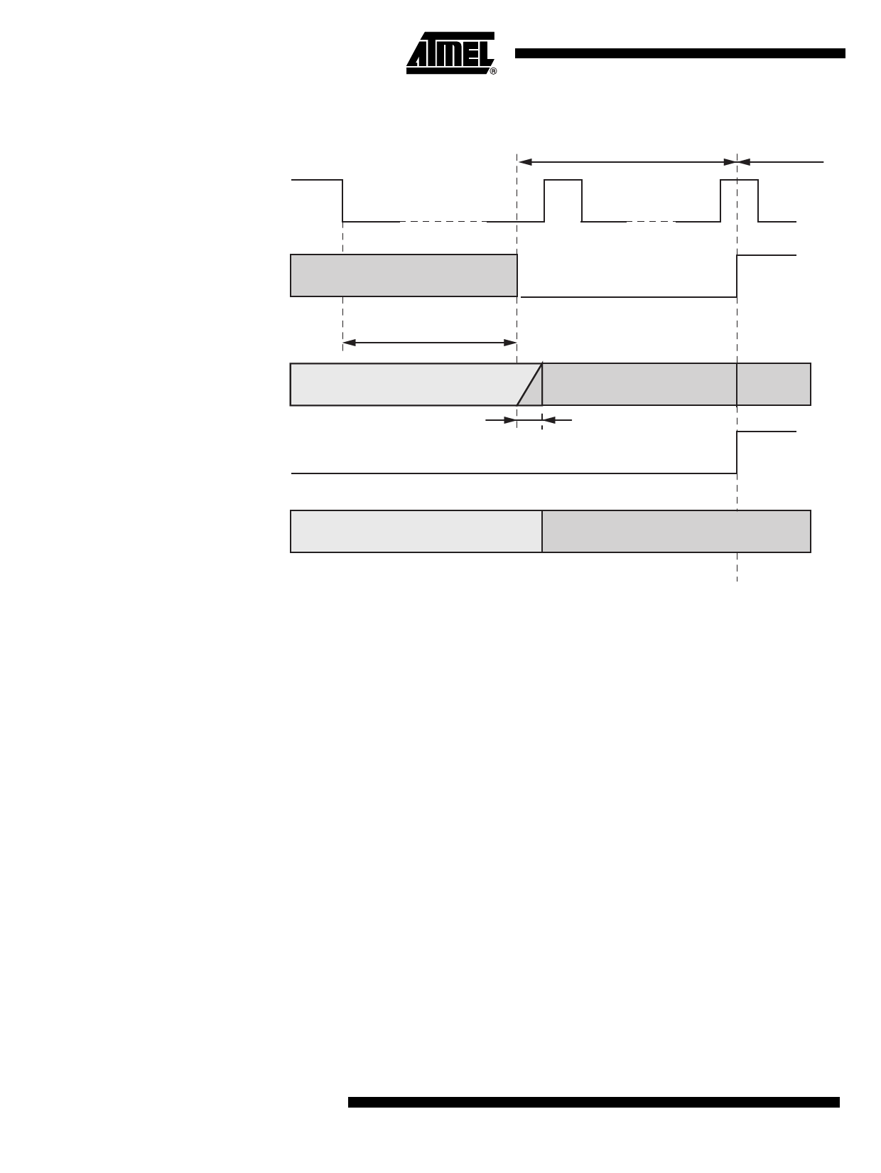
Figure 3-4. LIN Wake-up Waveform Diagram from Silent Mode
Pre-normal Mode
LIN Bus
VLIN < 0.4 VS
TXD
High
Normal Mode
RXD
VCC
High
Bus wake-up filtering time
tbus
Silent mode
Low
Pre-normal mode
EN
Node in Silent mode
Regulator Wake-up time
Normal mode
EN High
NRES If undervoltage, switch to Pre-normal Mode
Undervoltage detection active
3.3.14.3
Sleep Mode
The falling edge at EN has to occure not more than tDOMmin = 6 ms after or 3.2 µs before the fall-
ing edge at TXD in order to switch the IC into Sleep mode. The TXD Signal has to stay logic
low during the Mode Select window (see Figure 3-5 on page 11 and section “Silent Mode” on
page 8).
In Sleep mode the transmission path is disabled. Supply current from VBat is typically
IVSsleep = 10 µA. The VDD regulator is switched off. NRES and RXD are low. The internal slave
termination between pin LIN and pin VS is disabled to minimize the power dissipation in case pin
LIN is shorted to GND. Only a weak pull-up current (typically 10 µA) between pin LIN and pin VS
is present.
A falling edge at pin LIN followed by a dominant bus level maintained for a certain time period
(tbus) results in a remote wake-up request. The device switches from Sleep mode to Pre-normal
mode. The VDD regulator is activated and the internal LIN slave termination resistor is switched
on. The remote wake-up request is indicated by a low level at pin RXD to interrupt the microcon-
troller (see Figure 3-6 on page 12).
10 ATA6602/ATA6603
4921E–AUTO–09/09
Share Link: 