ATA6617 데이터 시트보기 (PDF) - Atmel Corporation
부품명
상세내역
제조사
ATA6617 Datasheet PDF : 308 Pages
| |||
2. Atmel ATA6616/ATA6617 LIN System in Package Solution (SIP)
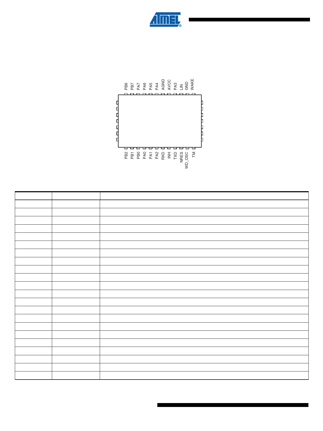
2.1 Pinning Atmel ATA6616/ATA6617
Figure 2-1. Pinning QFN38
PB5
PB4
VCC
GND
GND
GND
PB3
31 30 29 28 27 26 25 24 23 22 21 20
32
19
33
18
34
17
35 Atmel ATA6616/17 16
36
15
37
14
38
13
1 2 3 4 5 6 7 8 9 10 11 12
NTRIG
EN
VS
VCC
PVCC
KL15
MODE
Table 2-1. Pin Description
Pin
Symbol
Function
1
PB2
Port B 2 I/O line (PCINT10/OC1AV/USCK/SCL)
2
PB1
Port B 1 I/O line (PCINT9/OC1BU/DO)
3
PB0
Port B 0 I/O line (PCINT8/OC1AU/DI/SDA)
4
PA0
Port A 0 I/O line (PCINT0/ADC0/RXD/RXLIN)
5
PA1
Port A 1 I/O line (PCINT1/ADC1/TXD/TXLIN)
6
PA2
Port A 2 I/O line (PCINT2/ADC2/OC0A/DO/MISO)
7
RXD(1)
Receive data output
8
INH(1)
Battery-related output for controlling an external voltage regulator
9
TXD(1)
Transmit data input; active low output (strong pull down) after a local wake-up request
10
NRES(1)
Output undervoltage and watchdog reset (open drain)
11
WD_OSC(1)
External resistor for adjustable watchdog timing
12
TM(1)
For factory testing only (tie to ground)
13
MODE(1)
For debug mode: Low watchdog is on; high watchdog is off
14
KL_15(1)
Ignition detection (edge sensitive)
15
PVCC(1)
5V regulator sense input pin
16
VCC(1)
5V regulator output/driver pin
17
VS(1)
Battery supply
18
EN(1)
Enables the device into Normal Mode
19
NTRIG(1)
Low level watchdog trigger input from microcontroller
20
WAKE(1)
High voltage input for local wake-up request; if not needed connect to VS
21
GND(1)
System Ground LIN-SBC
22
LIN(1)
LIN bus line input/output
Note: 1. This identifies the pins of the LIN SBC Atmel® ATA6624
2 Atmel ATA6616/ATA6617
9132D–AUTO–12/10
Share Link: 