ATA6620 데이터 시트보기 (PDF) - Atmel Corporation
부품명
상세내역
제조사
ATA6620 Datasheet PDF : 20 Pages
| |||
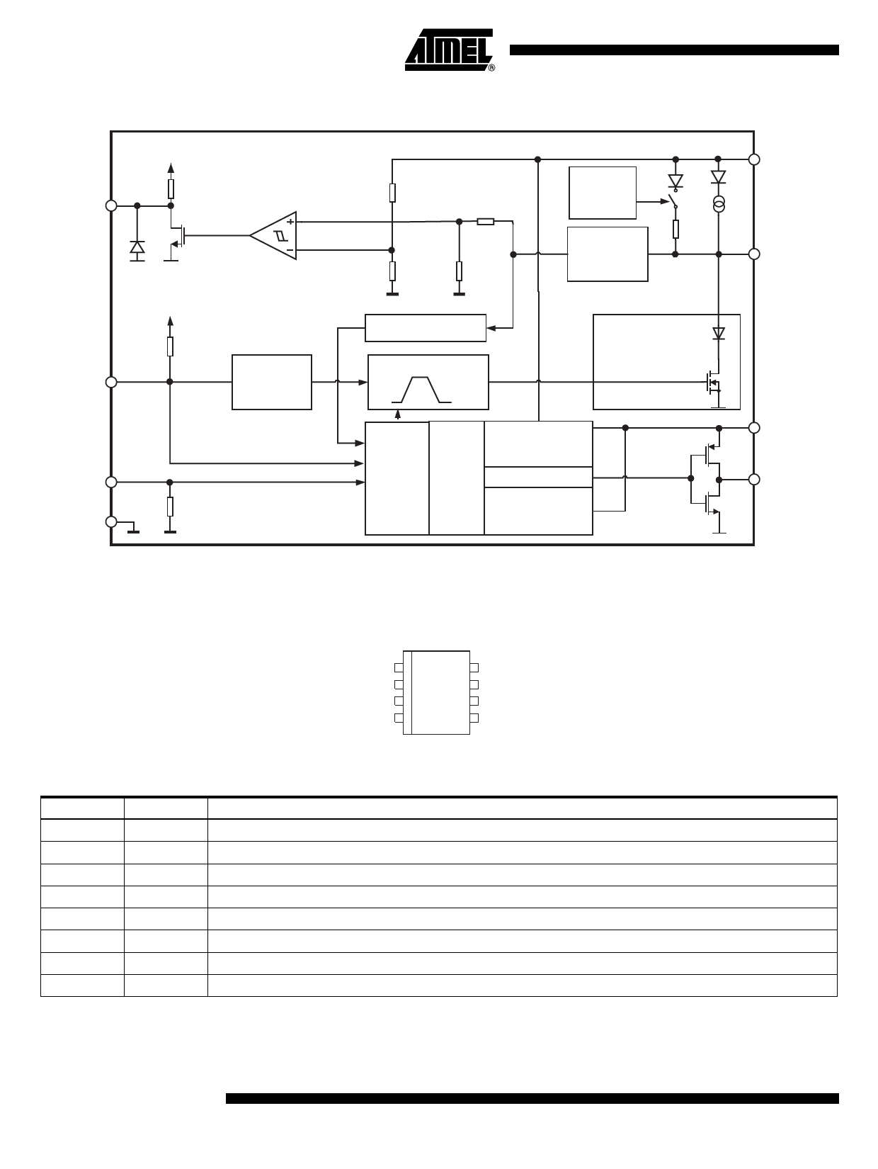
Figure 1-1. Block Diagram
VCC
ATA6620
RXD 5
Receiver
VCC
TXD
6
TXD
Time-out
Timer
EN 2
GND
3
2. Pin Configuration
Figure 2-1. Pinning SO8
Normal and
Pre-normal
Mode
Filter
1 VS
4 LIN
Wake-up Bus Timer
Slew Rate Control
Short Circuit and
Overtemperature
Protection
Control
Unit
Normal Mode
Sleep
Mode
Voltage Regulator
5V/50 mA/2%
VCC Undervoltage Reset
Switched Silent Mode
Off Voltage Regulator
5V/50 mA/7%
8 VCC
7 NRES
VS 1
EN 2
GND 3
LIN 4
8 VCC
7 NRES
6 TXD
5 RXD
Table 2-1.
Pin
1
2
3
4
5
6
7
8
Pin Description
Symbol Function
VS
Battery supply
EN
Enables Normal mode if the input is high
GND
Ground
LIN
LIN bus line input/output
RXD
Receive data output
TXD
Transmit data input
NRES Output undervoltage reset, low at reset
VCC
Output voltage regulator 5V/50 mA
2 ATA6620
4850D–AUTO–02/06
Share Link: 