ATA2526(2006) 데이터 시트보기 (PDF) - Atmel Corporation
부품명
상세내역
제조사
ATA2526 Datasheet PDF : 14 Pages
| |||
ATA2526
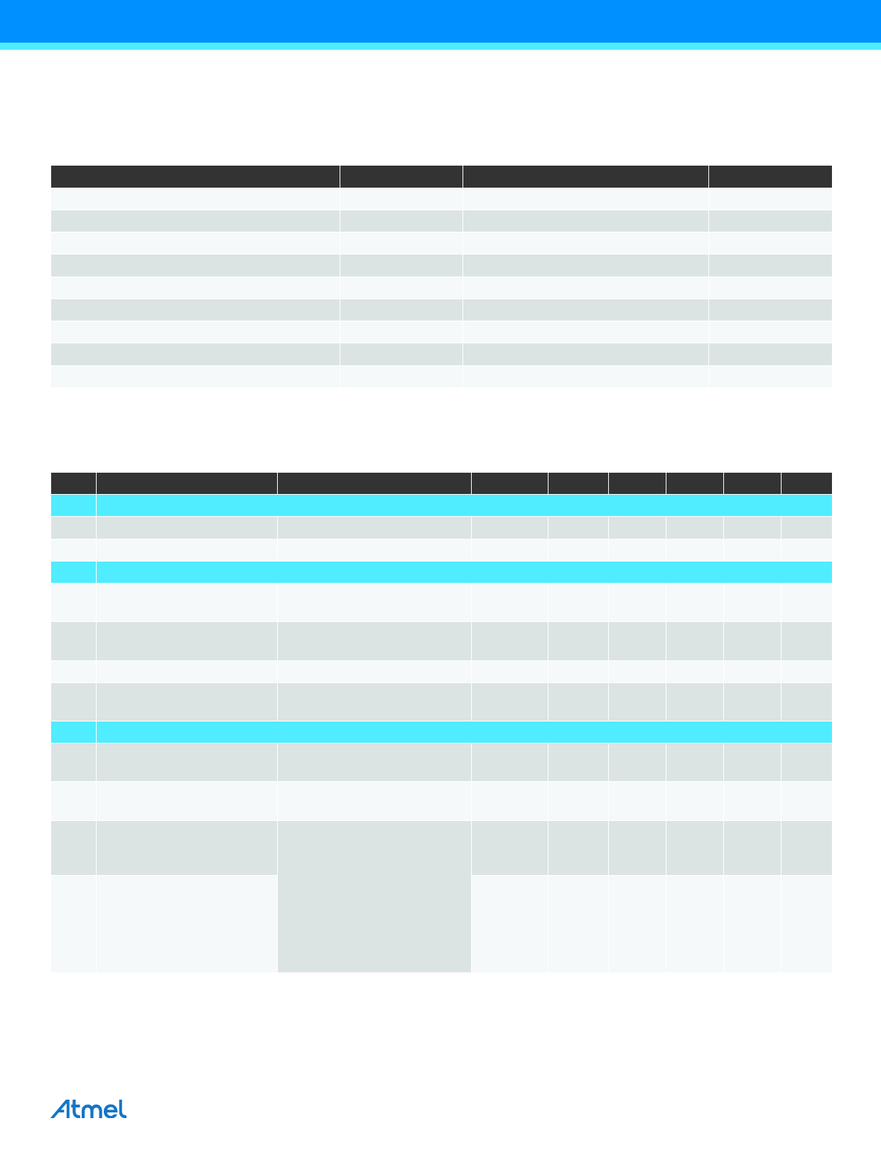
2. Absolute Maximum Ratings
Stresses beyond those listed under “Absolute Maximum Ratings” may cause permanent damage to the device. This is a stress rating
only and functional operation of the device at these or any other conditions beyond those indicated in the operational sections of this
specification is not implied. Exposure to absolute maximum rating conditions for extended periods may affect device reliability.
Parameter
Symbol
Value
Unit
Supply voltage
Supply current
Input voltage
Input DC current at VS = 5V
Output voltage
Output current
Operating temperature
Storage temperature
Power dissipation at Tamb = 25°C
VS
–0.3 to +6
V
IS
3
mA
VIN
–0.3 to VS
V
IIN
0.75
mA
VO
–0.3 to VS
V
IO
10
mA
Tamb
–25 to +85
°C
Tstg
–40 to +125
°C
Ptot
30
mW
3. Thermal Resistance
Parameters
Junction ambient TSSOP8
Symbol
RthJA
Value
110
Unit
K/W
4. Electrical Characteristics, 3-V Operation
Tamb = –25°C to +85°C, VS = 2.7V to 3.3V unless otherwise specified.
No. Parameters
Test Conditions
Pin
Symbol
Min.
Typ. Max. Unit Type*
1 Supply
1.1 Supply-voltage range
1.2 Supply current
2 Output
IIN =0
1
VS
2.7
3.0
3.3
V
C
1
IS
0.7
0.9
1.3
mA
B
2.1 Internal pull-up resistor
Tamb = 25°C
See Figure 6-10 on page 10
1, 3
RPU
40
kΩ
A
2.2 Output voltage low
R2 = 1.4 kΩ
See Figure 6-10 on page 10
3, 6
VOL
250
mV
B
2.3 Output voltage high
3, 1
2.4
Output current clamping
R2 = 0
See Figure 6-10 on page 10
3, 6
VOH
VS – 0.25
IOCL
8
VS
V
B
mA
B
3 Input
3.1 Input DC current
VIN = 0
See Figure 6-10 on page 10
5
IIN_DCMAX
–150
µA
C
3.2
Input DC current
VIN = 0; VS = 3V
See Figure 6-3 on page 7 Tamb = 25°C
5
IIN_DCMAX
–350
µA
B
*) Type means: A =100% tested, B = 100% correlation tested, C = Characterized on samples, D = Design parameter
Notes: 1. BER = bit error rate; e.g., BER = 5% means that with P = 20 at the input pin 19...21 pulses can appear at the pin OUT
2. After transformation of input current into voltage
3
4905D–AUTO–10/06
Share Link: 