ATC13 데이터 시트보기 (PDF) - Atmel Corporation
부품명
상세내역
제조사
ATC13 Datasheet PDF : 12 Pages
| |||
optimization. Built-in self-test (BIST) interface allows for easy connection to most mem-
BIST solutions. The special test modes allow externally bypassing read self-timed
circuits and adjusting read margins. Within limits, the user has flexibility in specifying the
logical size of the ROM, including word size, number of address locations and column
mux.
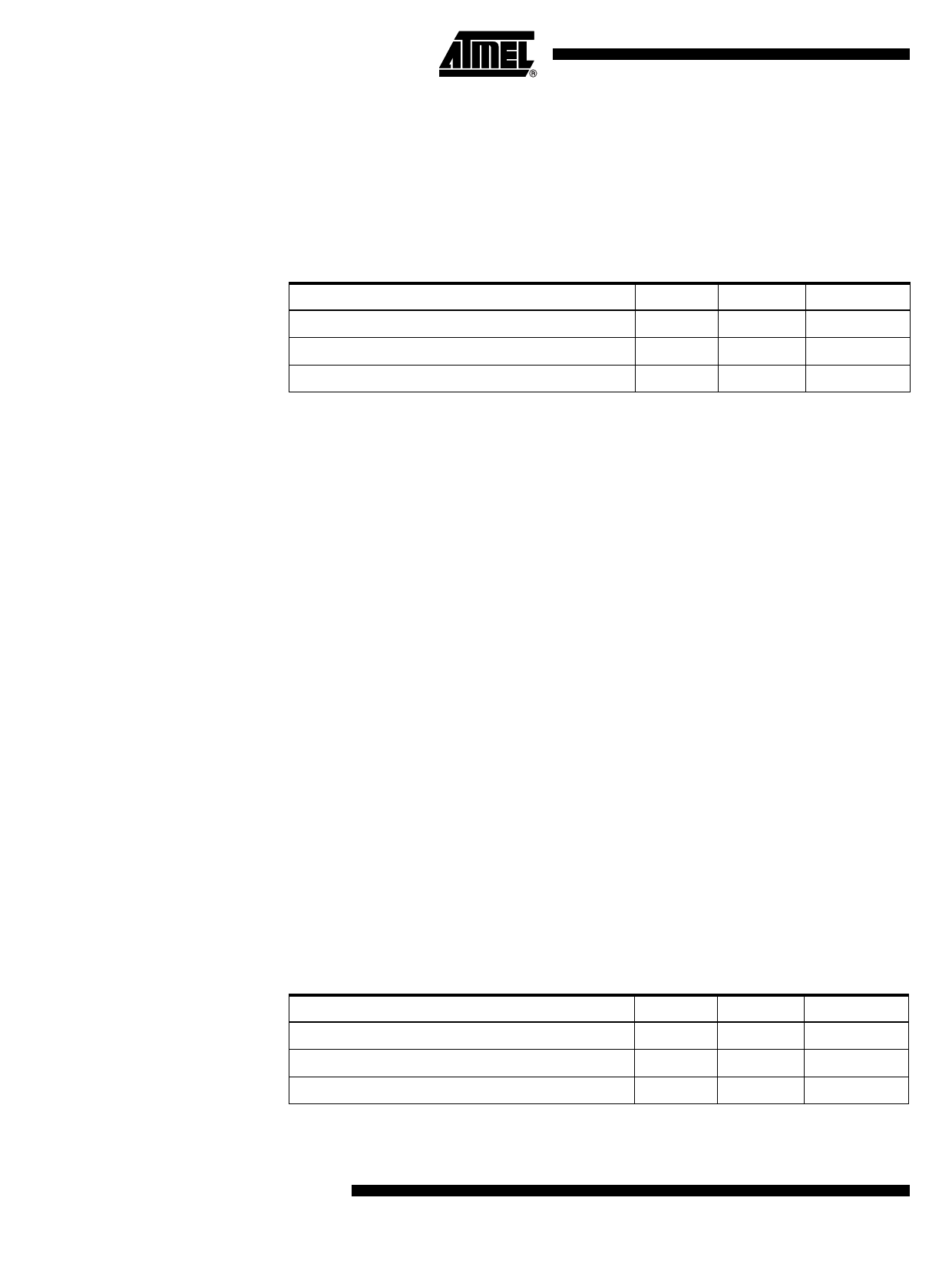
Table 7-3 gives the range of permitted via programmable ROM configurations.
Table 7-3. Configuration Range
Parameter
Min
Address Locations (words)
256
Word Size (Number of I/O bits)
4
Total Bits in Core (Word Size x Address Locations)
512
Max
64K
64
1M
Increment
16 x CM(1)
2 bits
Note: 1. CM = 16, 32, 64: Column Mux option
7.4 Two-port Synchronous Register File
Key features of the two-port synchronous register file are:
• 2-Port (1R, 1W) high-speed/low-power Register File
• 600 MHz worst-case cycle time for 32 words x 32 bits
• Zero quiescent current
• 3-state outputs
• Several aspect ratios for optimization of performance
• Separate data-in, data-out pins
• Optional sub-word write capability
The two-port synchronous register file compiler is a 2-port (one for write, one for read)
memory. This is a high-speed/low-power synchronous register file compiler. The quies-
cent current consumption is zero when all Register File inputs (including CLKA and
CLKB) are stable. The compiler is optimized for a power supply voltage range of 1.1V to
1.32V and can operate at voltages as low as 1.0V. The Register File instances can be
built with several aspect ratios for maximum area and performance optimization. Sepa-
rate clocks (CLKA, CLKB), output (QB), and input (DA) pins allow independent read and
write cycles. Built-in self-test BIST interface allows for easy connection to most mem-
BIST solutions. The memory also also includes a bit-write feature where selective write
to each I/O can be done. A maskable write enable signal is provided for each I/O for
maximum flexibility. Within limits, the user has flexibility in specifying the logical size of
the Register File, including word size, number of address locations and column mux.
Table 7-4 gives the range of permitted two-port synchronous register file configurations.
Table 7-4. Configuration Range
Parameter
Min
Address Locations (words)
8
Word Size (Number of I/O bits)
2
Total Bits in Core (Word Size x Address Locations)
16
Max
1024
256
16K
Increment
1 x CM(1)
1 bit
Notes: 1. CM = 1, 2, 4: Column Mux option
10 ATC13 Summary
6134AS–CASIC–08-Mar-05
Share Link: 