AWC6323 데이터 시트보기 (PDF) - ANADIGICS
부품명
상세내역
제조사
AWC6323 Datasheet PDF : 11 Pages
| |||
AWC6323
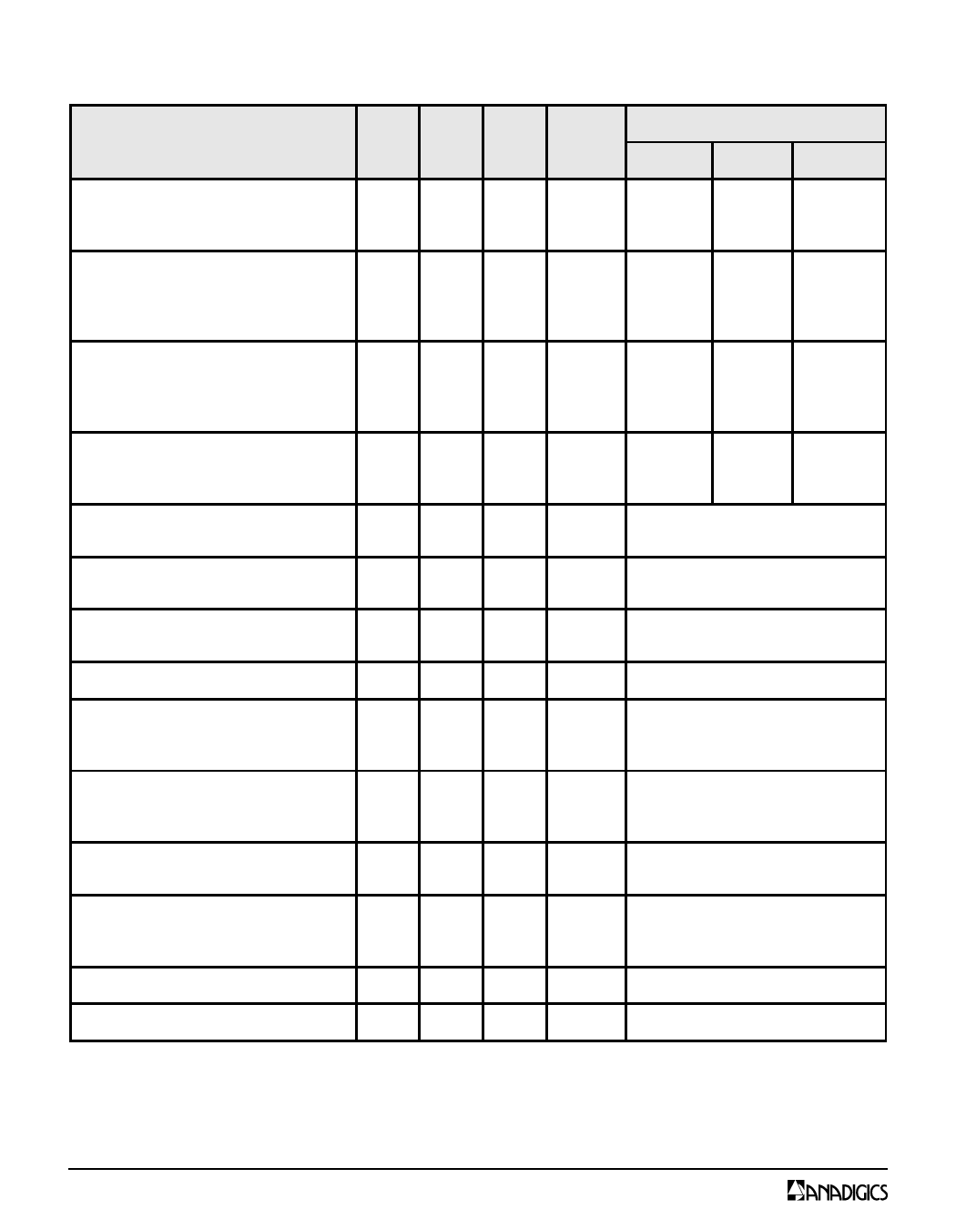
Table 5a: Electrical Specifications - PCS Band (BC 1)
(TC = +25 °C, VBATT = VCC = +3.4 V, VEN_PCS = +1.8 V, 50 Ω system, CDMA2000 RC-1 waveform)
PARAMETER
MIN TYP MAX UNIT
COMMENTS
VMODE1
VMODE2
POUT
Gain
Adjacent Channel Power
at 1.25 MHz offset (1)
Primary Channel BW = 1.23 MHZ
Adjacent Channel BW = 30 kHz
Adjacent Channel Power
at 1.98 MHz offset (1)
Primary Channel BW = 1.23 MHZ
Adjacent Channel BW = 30 kHz
Power-Added Efficiency (1)
Quiescent Current (Icq)
Mode Control Current
Battery Current
24.5 26.5 30
10 13.5 16
7
10
13
0V
1.8 V
dB 1.8 V
1.8 V
0/1.8 V 0 V
+27.9 dBm
+16 dBm
+10 dBm
-
-51 -46.5
0V
1.8 V
+27.9 dBm
-
-52 -46.5
dBc 1.8 V
1.8 V
+16 dBm
-
-52 -46.5
0/1.8 V 0 V
+10 dBm
-
-56
-54
-
-59
-54
-
-63
-54
33 36.5
-
18
21
-
8
11
-
-
3.5
6
-
0.05 0.1
-
1
2
0V
dBc
1.8 V
0/1.8 V
1.8 V
1.8 V
0V
+27.9 dBm
+16 dBm
+10 dBm
0V
1.8 V
% 1.8 V
1.8 V
0/1.8 V 0 V
+27.9 dBm
+16 dBm
+10 dBm
mA
through VBATT and VCC pins,
VMODE1 = 0/1.8 V, VMODE2 = 0 V
mA
tthrough VMODE pins,
VMODE1 = 0/1.8 V, VMODE2 = 0 V
mA
through VBATT pin, VMODE1 = 0/1.8 V,
VMODE2 = 0 V
Enable Current
-
<0.1 0.15
mA
through VEN_CELL pin
Total Decoder Current on VBATT
(in Shutdown mode)
Total PA Leakage Current on VCC
(in Shutdown mode)
Noise in Receive Band(2)
Harmonics
2fo
3fo, 4fo
VBATT = +4.2 V, VCC = +4.2 V,
-
7
16
A
V = EN_CELL 0 V,
VMODE1 = 0 V, VMODE2 = 0 V
VBATT = +4.2 V, VCC = +4.2 V,
-
1
5
A
V = EN_CELL 0 V,
VMODE1 = 0 V, VMODE2 = 0 V
-
-
-133
-137
-131
-134
dBm/Hz
VMODE1 = 0 V, VMODE2 = 1.8 V
VMODE1 = VMODE2 = 1.8 V
-
-
-41 -30
-50
-30
dBc POUT < +27.9 dBm
Input Impedance
-
-
2:1 VSWR
Coupling Factor
-
22
-
dB
6
Data Sheet - Rev 2.2
03/2012
Share Link: 