AWT6105 데이터 시트보기 (PDF) - ANADIGICS
부품명
상세내역
제조사
AWT6105 Datasheet PDF : 16 Pages
| |||
AWT6105
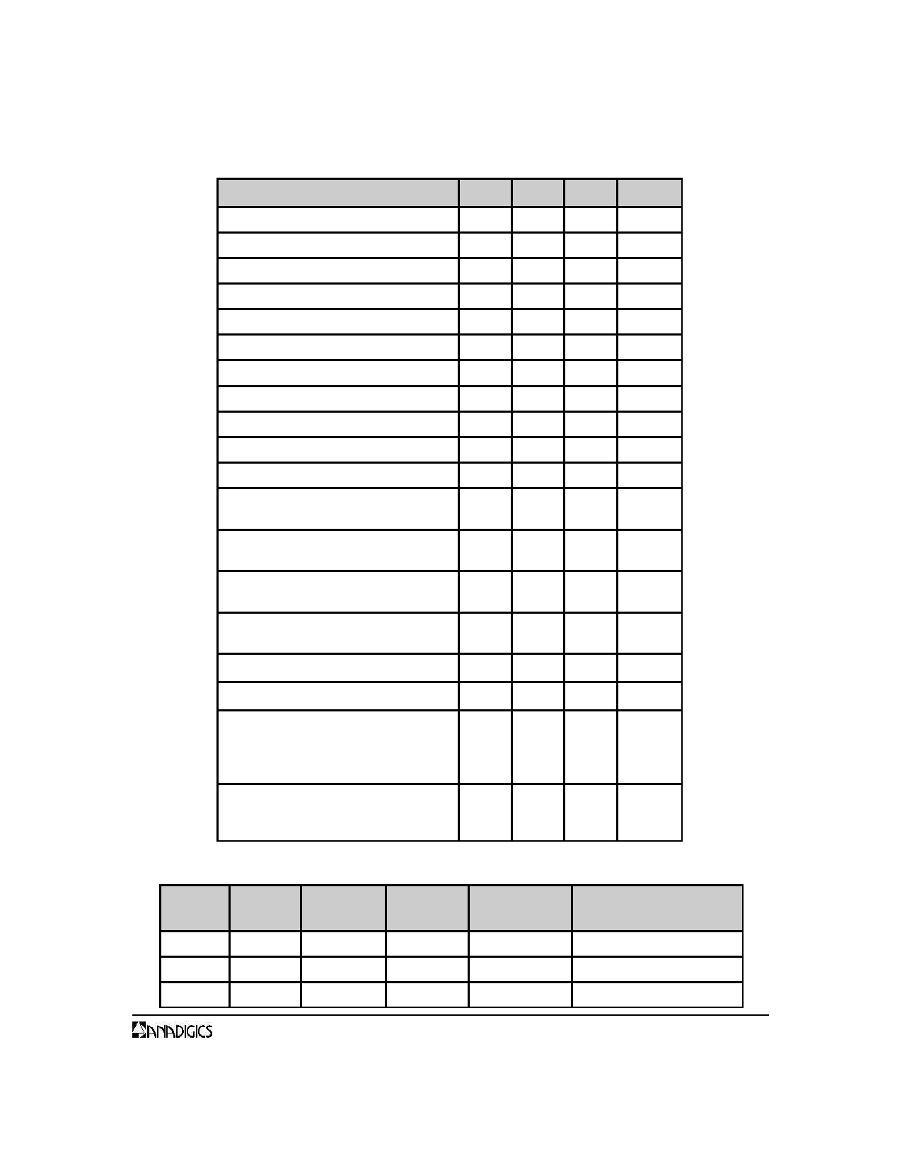
Table 3: Electrical Specifications (AMPS 824-849 MHz)
PARAMETER
MIN TYP MAX UNIT
Frequency Range
824
849
MHz
Supply Voltage Range
3.0
3.5
4.2
V
Ref Voltage Range: PA "on"
2.9
3.0
3.1
V
Ref Voltage Range: PA "off"
0
0.5
V
Ref current
5
7
mA
V High Bias
MODE
VMODE Low Bias
Gain, POUT= 31 dBm
Output Power, VCC = 3.5V
Output Power, VCC = 3.0V
Input Impedance
0
0.5
V
2.5
3
3.1
V
28
31
dB
31
32
dBm
30
dBm
2:1
Ratio
Power Added Efficiency
POUT = 31dBm Vcc=3.5V, VMODE = 2.7V
46
%
Icq (VMODE= 2.7V)
Low Power Mode
50
mA
Noise at Receiver Band
POUT ≤ 31 dBm
Leakage Current
V = 3.5V ; V = 0V ; V = 0V
CC
REF
MODE
Harmonics 2fo, P = 31 dBm
OUT
3fo, P = 31 dBm
OUT
Stability
(out of band load VSWR ≤ 8:1)
(in band load VSWR ≤ 8:1)
Over Temperature and & Voltage
-135
dBm/Hz
5
µA
-40 -30
dBc
-50 -30
dBc
dBc, all
-70
spurious
P
OUT
≤
31dBm
Ruggedness
Stress for no permanent degradation or 8:1
failure, VCC = 5.0 Over Temperature
Ratio
Note:
Unless
otherwise
specified:
Vcc
=
3.5V,
Z
IN
=
Z
OUT
=
50Ω
System
,
TC
=
25
°C
Table 4: Bias Control
Bias
Mode
VMODE
ICQ TYP
POWER
RANGE
POUT LEVELS
MODE
Low
2.7V
50 mA
All
0-32 dBm
AMPS All Power Levels
Low
2.7V
50 mA
Low
-50 to +20 dBm
CDMA Low Power
High
0V
100 mA
High
20-29 dBm
CDMA High Power
PRELIMINARY DATA SHEET - Rev 1.2
3
10/2001
Share Link: 