AWT6113 데이터 시트보기 (PDF) - ANADIGICS
부품명
상세내역
제조사
AWT6113 Datasheet PDF : 16 Pages
| |||
AWT6113
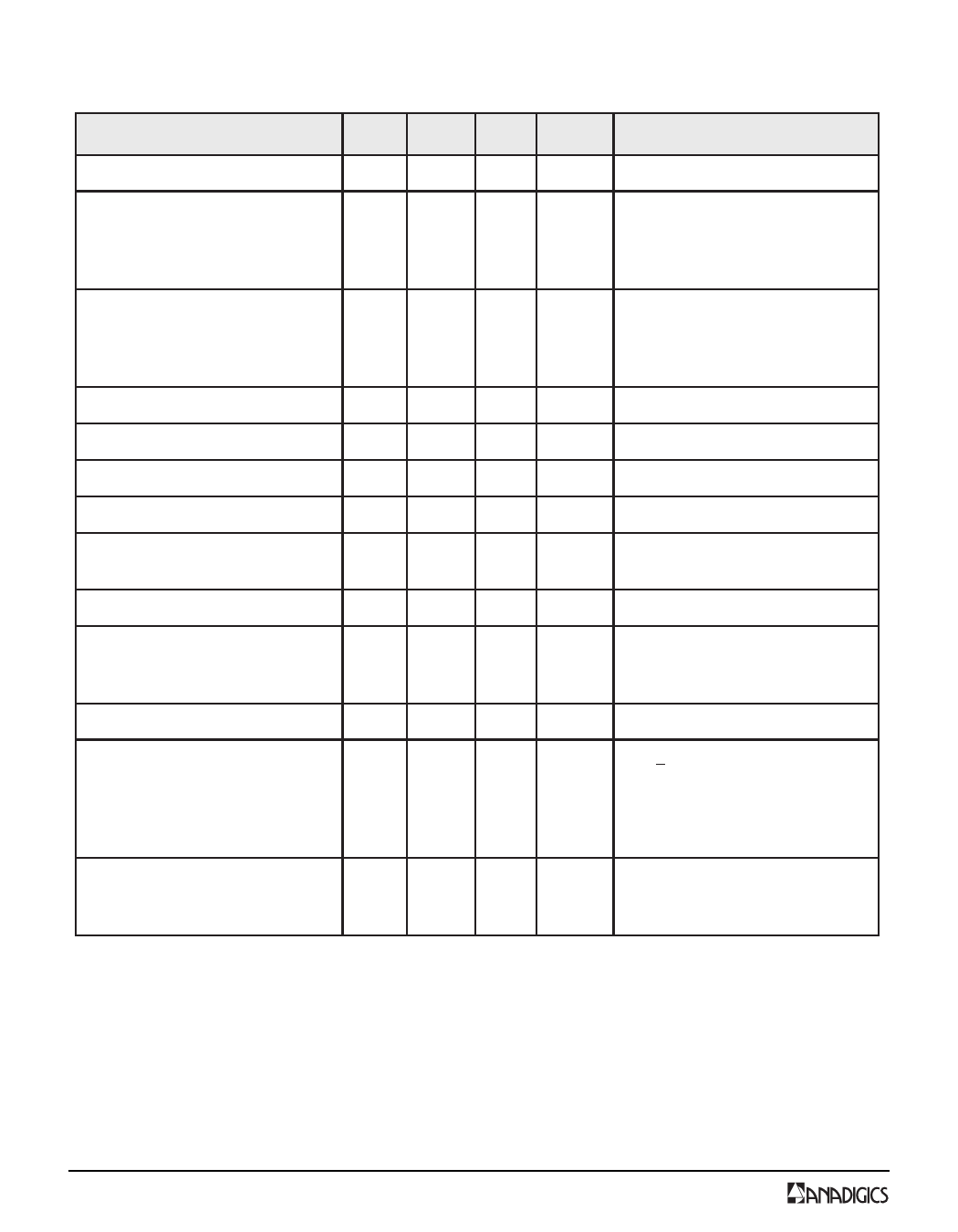
Table 4: Electrical Specifications - High Bias Mode
(TC = +25 °C, VCC = +3.4 V, VREF = +2.85 V, VMODE = 0 V, POUT = +28 dBm, 50 Ω system)
PARAMETER
MIN TYP MAX UNIT
COMMENTS
Gain
26
28
30
dB
Adjacent Channel Power (1)
at ±1.25 MHz offset
Primary Channel BW = 1.23 MHz
-
Adjacent Channel BW = 30 kHz
-50
-47
dBc
Adjacent Channel Power
at ±2.25 MHz offset
Primary Channel BW = 1.23 MHz
-
Adjacent Channel BW = 30 kHz
-61 -57
dBc
Power-Added Efficiency (1)
36.5 38
-
%
Quiescent Current
-
70
90
mA
Reference Current
Mode Control Current
Leakage Current
Noise in Receive Band
-
6
8
mA through VREF pin
-
0
-
mA through VMODE pin
-
<1
5
µA
VCC = +4.2 V, VREF = 0 V
VMODE = 0 V
-
-135 -133 dBm/Hz 1930 MHz to 1990 MHz
Harmonics
2fo
3fo
-
-
-46
-52
-30
-30
dBc
Input Impedance
-
-
2:1 VSWR
Spurious Output Level
(all spurious outputs)
POUT <+28 dBm
In-band load VSWR < 8:1
-
-
-65
dBc Out-of-band load VSWR < 8:1
Applies over all voltage and
temperature operating ranges
Load mismatch stress with no
permanent degradation or failure
8:1
-
Notes:
(1) PAE and ACP limit applies to 1880 MHz.
VCC = +5.0 V, PIN = +5 dBm
- VSWR Applies over full operating
temperature range
4
PRELIMINARY DATA SHEET - Rev 1.4
12/2002
Share Link: 