AWT6168 데이터 시트보기 (PDF) - ANADIGICS
부품명
상세내역
제조사
AWT6168 Datasheet PDF : 12 Pages
| |||
AWT6168
GSM/GPRS/Polar EDGE Power Amplifier
Module with Integrated Power Control
ADVANCED PRODUCT INFORMATION - REV 0.1
FEATURES
• Internal Reference Voltage
• Integrated Power Control Scheme
• InGaP HBT Technology
• ESD Protection on All Pins (2.5 kV)
• Low profile 1.3 mm
• Small Package Outline 7 mm x 7 mm
• EGPRS Capable (class 12)
GMSK MODE
• Integrated power control (CMOS)
• +35 dBm GSM850/900 Output Power
• +33 dBm DCS/PCS Output Power
• 55 % GSM850/900 PAE
• 50 % DCS/PCS PAE
• Power control range > 50 dB
EDGE MODE
• +30.5 dBm GSM850/900 Output Power
• +29.5 dBm DCS/PCS Output Power
• 25 % GSM850/900 PAE
• 25 % DCS/PCS PAE
APPLICATIONS
• GSM850/GSM900/DCS/PCS Handsets
• Dual/Tri/Quad Band PDA
• GMSK and 8-PSK Polar Modulation
Schemes
DCS/PCS_IN
DCS/PCS
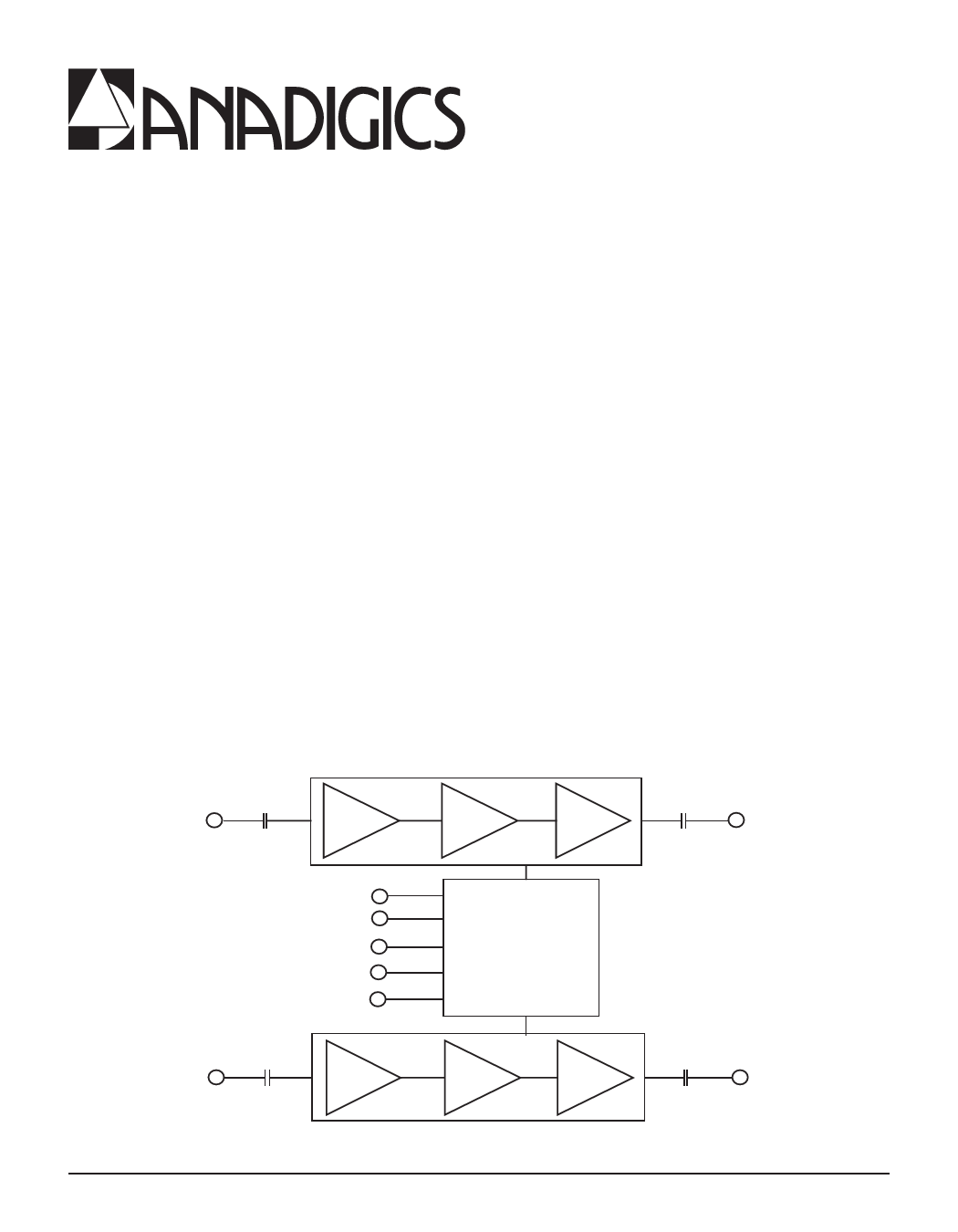
PRODUCT DESCRIPTION
This power amplifier module supports dual, tri and
quad band applications for GMSK and 8-PSK modu-
lation schemes using a polar architecture. There are
two amplifier chains, one to support GSM850/900
bands, the other for DCS/PCS bands.
The module includes an internal reference voltage
and integrated power control scheme for use in both
GMSK and 8-PSK operation. This facilitates fast and
easy production calibration and reduces the num-
ber of external components required to complete a
power control function. The amplifier’s power con-
trol range is typically 55 dB, with the output power set
by applying an analog voltage to VRAMP.
All of the RF ports for this device are internally
matched to 50 Ω . Internal DC blocks are provided at
the RF inputs.
DCS/PCS_OUT
BS
TX_EN
VBATT
CEXT
VRAMP
Bias/Power
Control
GSM850/900_IN
GSM850/900
Figure 1: Block Diagram
01/2005
GSM850/900_OUT
Share Link: 