AZ100LVEL33 데이터 시트보기 (PDF) - Arizona Microtek, Inc
부품명
상세내역
제조사
AZ100LVEL33 Datasheet PDF : 8 Pages
| |||
AZ100LVEL33
ARIZONA MICROTEK, INC.
ECL/PECL ÷4 Divider
FEATURES
PACKAGE AVAILABILITY
Green / RoHS Compliant /
Lead (Pb) Free package available
Operating Range of 3.0V to 5.5V
PACKAGE
MLP 8 (2x2) Green
/ RoHS Compliant /
Lead (Pb) Free
PART NUMBER
AZ100LVEL33NG
MARKING
C3G
<Date Code>
NOTES
1,2
470ps Propagation Delay
SOIC 8 Green /
5.0+ GHz Toggle Frequency
RoHS Compliant /
Internal Input Pulldown Resistors
Lead (Pb) Free
MSOP 8 Green /
Direct Replacement for ON Semiconductor RoHS Compliant /
MC100EL33 & MC100LVEL33
Lead (Pb) Free
AZ100LVEL33DG
AZ100LVEL33TG
AZM100G
LVEL33
AZHG
LV33
1,2,3
1,2,3
Transistor Count = 91 Devices
1 Add R1 at end of part number for 7 inch (1K parts), R2 for 13 inch (2.5K
IBIS Model Files Available on Arizona
Microtek Web Site
>2 kV HBM ESD Protection
parts) Tape & Reel.
2 Date code format: “Y” or “YY” for year followed by “WW” for week.
3 Date code “YWW” or “YYWW” on underside of part.
Additional ESD Data Available on
Arizona Microtek Website
DESCRIPTION
The AZ100LVEL33 is an integrated ÷4 divider. The RESET pin is asynchronous and clears the output (Q Low,
Q¯ High) on the rising edge. Upon power-up, the internal flip-flop will be in a random logic state. RESET allows for
the synchronization of multiple LVEL33’s in a system.
The LVEL33 provides a VBB output for single-end use or a DC bias reference for AC coupling to the device.
For single-ended input applications, the VBB reference should be connected to one side of the CLK/ C¯¯L¯K¯ differential
input pair. The input signal is then fed to the other CLK/ C¯¯L¯K¯ input. The VBB pin can support 1.0mA sink/source
current. When used, the VBB pin should be bypassed to ground via a 0.01F capacitor.
NOTE: Specifications in the ECL/PECL tables are valid when thermal equilibrium is established.
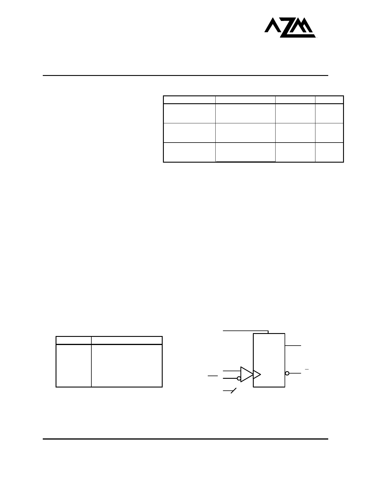
PIN DESCRIPTION
PIN
CLK, C¯L¯¯K
RESET
VBB
Q, Q¯
VCC
VEE
FUNCTION
Clock Inputs
Asynchronous Reset
Reference Voltage Output
Data Outputs
Positive Supply
Negative Supply
RESET
CLK
CLK
VBB
LOGIC DIAGRAM
R
Q
÷4
Q
1630 S. STAPLEY DR., SUITE 127 MESA, ARIZONA 85204 USA (480) 962-5881 FAX (623) 505-2414
www.azmicrotek.com
Share Link: 