LB1881M 데이터 시트보기 (PDF) - SANYO -> Panasonic
부품명
상세내역
제조사
LB1881M Datasheet PDF : 6 Pages
| |||
Continued from preceding page.
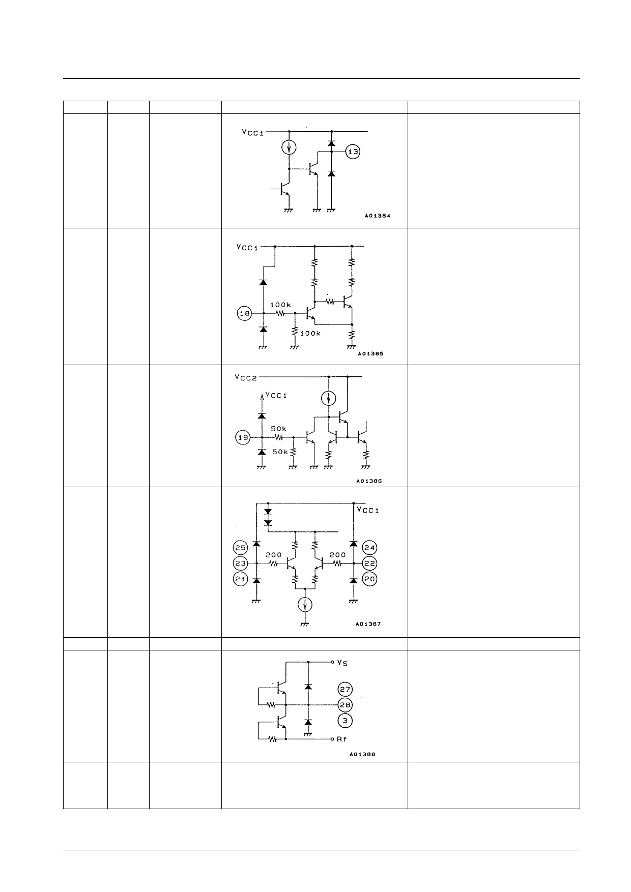
Pin No. Symbol
Pin voltage
13
FGOUT2
LB1881M
Equivalent circuit
Unit (resistance: Ω)
Pin function
FG Schmitt amplifier output pin
18
FRC (H): 2.8 V min
(L): 1.2 V max
(When VCC1 is 5 V)
19
BR
(H): 2.0 V min
(L): 0.8 V max
20
WIN2 1.4 V min
21
WIN1 2.8 V max
22
23
VIN2
VIN1
(When VCC1 is 5 V)
24
UIN2
25
UIN1
26
Rf
27
UOUT
28
VOUT
3
WOUT
1, 2,
14, 15,
16, 17,
29, 30
FRAME
(GND)
Pin for setting the motor to forward or reverse
rotation
Low level: Forward rotation
(under 1.2 V: when VCC1 is 5 V)
High level: Reverse rotation
(over 2.8 V: when VCC1 is 5 V)
Motor brake pin
Low level: Motor drive
(under 0.8 V)
High level: Motor brake
(over 2.0 V)
W phase Hall element input pins.
Logic high is defined to be states where
WIN1 > WIN2.
V phase Hall element input pins.
Logic high is defined to be states where
VIN1 > VIN2.
U phase Hall element input pins.
Logic high is defined to be states where
UIN1 > UIN2.
Output transistor GND
Output pin
GND for all circuits other than output transistors.
No. 4455-5/6
Share Link: 