SA57000-25 데이터 시트보기 (PDF) - Philips Electronics
부품명
상세내역
제조사
SA57000-25
Philips Electronics

SA57000-25 Datasheet PDF : 8 Pages
| |||
Philips Semiconductors
CapFREE™ 150 mA, low-noise, low dropout regulator
with thermal protection
Product data
SA57000-XX
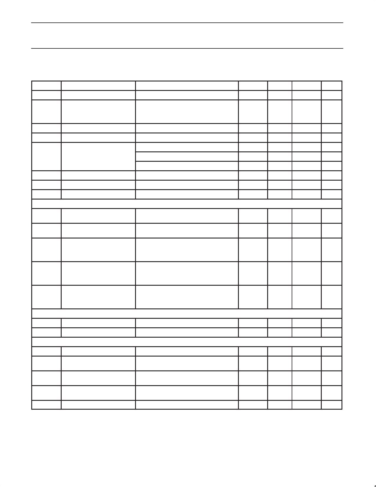
CHARACTERISTICS
VIN = VOUT(nom) + 0.5 V. (Note 1.)
SYMBOL
PARAMETER
CONDITIONS
MIN.
TYP.
MAX.
UNIT
VIN
input voltage
output voltage accuracy 2
ILIM
current limit
IQ
ground pin current
dropout voltage 3
∆VLNR
∆VLDR
en
Shutdown
line regulation
load regulation
output voltage noise
IOUT = 1 mA
Tamb = +25 °C
–40 °C ≤ Tamb ≤ +85 °C
IOUT = 1 mA to 150 mA
IOUT = 1 mA
IOUT = 50 mA
IOUT = 150 mA
VIN = (VOUT + 0.1 V) to 5.5 V; IOUT = 20 mA
IOUT = 1 mA to 150 mA
f = 10 Hz to 100 kHz, COUT = 10 µF
VOUT(nom)
–
–2.0
160
–
–
–
–
–
–
–
–
±1
–
300
85
1
55
165
–
0.01
30
5.5
V
–
%
2.0
%
–
mA
150
µA
–
mV
120
mV
–
mV
0.1
%/V
0.02
%/mA
–
µVRMS
VIH
PWRON input threshold
(HIGH ON-state)
VIN → VOUT(nom) → 5.5 V
0.7 × VIN
–
–
V
VIL
PWRON input threshold
(HIGH ON-state)
VIN → VOUT(nom) → 5.5 V
–
–
0.3 × VIN
V
IPWRON
PWRON input bias current
IQ(SHDN) shutdown supply current
tPWRON
power-on start-up time 4
Thermal protection (Note 2)
VPWRON = VIN
Tamb = +25 °C
Tamb = +85 °C
VOUT = 0 V
Tamb = +25 °C
Tamb = +85 °C
IOUT = 1 mA, COUT = 100 nF
Tamb = +25 °C
Tamb = –40 to +85 °C
–
0.01
1
µA
–
0.05
–
µA
–
0.05
1
µA
–
0.2
1
µA
–
25
100
µs
–
35
200
µs
TSHDN
thermal shut-down temperature
∆TSHDN
thermal shut-down hysteresis
PWROK output (power and temperature OK) (Note 2)
–
144
–
°C
–
13
–
°C
PWROK trip temperature
–
127
–
°C
PWROK trip temperature
hysteresis
–
12
–
°C
PWROK trip as percentage of
VOUT(nom)
–3.5
–6
–8
%
PWROK hysteresis as
percentage of VOUT(nom)
–
2
–
%
PWROK output (when tripped)
ISINK = 0.5 mA
–
0.1
0.4
V
NOTES:
1. Limits are production tested at Tamb = +25 °C. All devices are 100% production tested at 25 °C. Limits over the operating tempreature are
guaranteed by design.
2. Accuracy ±2 °C over temperature range guaranteed by design and characterization.
3. The dropout voltage is defined as VIN – VOUT, where VOUT is 100 mV below the value of VOUT for VIN = VOUT + 0.5 V..
4. Time needed for VOUT to reach 95% of VOUT(nom).
2001 Aug 27
4
Share Link: