BIT3193 데이터 시트보기 (PDF) - Unspecified
부품명
상세내역
제조사
BIT3193 Datasheet PDF : 10 Pages
| |||
Beyond Innovation Technology Co., Ltd.
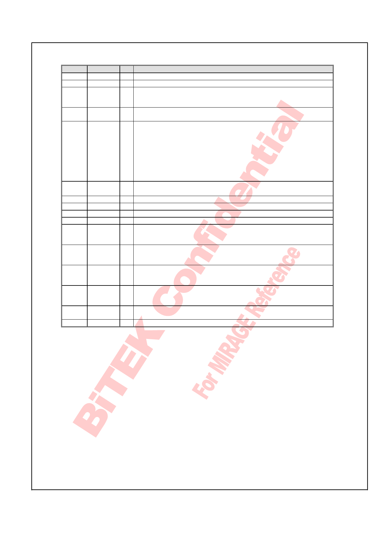
Pin Description:
BIT3193
Pin No.
1
2
3
4
5
6
7
8
9
10
11
12
13
14
15
16
Symbol
INN
CMP
LOAD
CTOSC
TIMER
ONOFF
GND
NOUT2
NOUT1
VDD
PWMOUT
CTPWM
PWMDC
CLAMP
ISEN
MODSEL
I/O
Descriptions
I The inverting input of the error amplifier.
O Output of the error amplifier.
A switch that connected to the high frequency triangle wave generator.
I/O This switch is open while ISEN pin <1.3V. An external resistor connected
here may change the operation frequency of CTOSC in open load situation.
I/O
An external capacitor connected here can set the frequency of high frequency
PWM controller.
With internal reference current and an external capacitor connected here can
set the required period of starting and the timing of initialization. The
controller is forced to reset mode while TIMER <0.3V. During reset mode, a ~
60uA current will flow into the INN pin to reduce the output level of the error
I/O amplifier CMP to turn off the controller. The latched off protection function will
be enabled after this node is charged to > 2.5V. System is latched off if any
abnormal operation is detected if pin TIMER > 2.5V.
The output current of this pin is 20uA when TIMER < 0.3V.
The output current becomes to 1uA when TIMER > 0.3V
I
The control pin of turning on or off the IC. 1V threshold with an internal 80K±
15% ohm pull-low resistor.
I/O The ground pin of the device.
O The number 2 output driver for driving the NMOSFET switch.
O The number 1 output driver for driving the NMOSFET switch.
I The power supplies pin of the device.
The output pin of low frequency PWM generator. A 2.5V or floating two state
O output is provided through this pin.
The internal circuit limits the max. Duty-cycle to ~ 92%.
With the internal reference current and an external capacitor connected here
I/O can set the operation frequency of low frequency PWM generator with 1.0V ~
2.5V triangle wave output.
Low frequency PWM controlling input. A PWM output comes out by
I comparing this DC input and the 1.0 ~ 2.5V triangle wave that is generated
by CTPWM.
Over voltage clamping. If a > 2.0 V voltage is detected. A ~ 60uA current will
I flow into the INN pin to reduce the output of the error amplifier pin CMP to
regulate the output voltage.
I
Load current detection pin, the open load situation is detected if a less than
1.3V input is sensed.
O To set the output polarity of the low frequency PWM controller.
04/11/08
Confidential, for authorized user only
page 3 of 10
Share Link: 