BL34018 데이터 시트보기 (PDF) - Shanghai Belling Co., Ltd.
부품명
상세내역
제조사
BL34018 Datasheet PDF : 16 Pages
| |||
Delta RXO, TXO Voltages
Speaker Amp Gain
Microphone Amp Gain
Microphone Amp Input Resistance
Tx - Rx Switching Threshold (@ 20 uA)
4,26
15,19
9,10
9
5,7
BL34018
±0.24
±0.003
±0.001
+0.4
±0.2
%/°C
dB/°c
dB/°c
%/°c
nA/°c
6. DESIGN GUIDELINES(REF TO FIG. 1)
ATTENUATORS
The transmit and receive attenuators are complementary in function, i.e., when one is at
maximum gain the other is at maximun attenuation, and vice versa. They are never both on or both
off. Their main purpose is to control the transmit and receive paths to provide the half-duplex
operation required of a speakerphone. The attenuators are controlled safely by the voltage at the
ACF pin. The ACF voltage is provided by the Attenuator Control block, which receives 3 inputs:a)
the TX - RX Comparator, b) the Transmit Detector Comparator, and c) the Volume Control. The
response of the attenuators is based on the difference of the ACF voltage from VCC (referred to as
∆Vacf). If ∆Vacf is approximately 6mV the transmit attenuator is fully on and the receive attenuator
is fully off( transmit mode). If ∆Vacf is approximately 150mV the circuit is in the receive mode. If
∆Vacf is approximately 75mV, the circuit is in the idle mode, and the two attenuators are at gain
settings approximately half way (in dB) between their fully on and fully off positions.
The maximum gain and attenuation values are determined by the three external resistors RR,
RTX, and RRX. RR affects both attenuators according to its value RELATIVE to RTX and RRX.
RTX affects the gain and attenuation of only the transmit attenuator, while RRX affects the gain and
attenuation of only the receive attenuator. A value of 30 k is recommended for RR as a starting point,
and then RTX and RRX selected to suit the particular design goals.
The input impedance of the attenuators (at TXI and RXI) is typically 5.0 kΩ, and the
maximum input signal which will not cause output distortion is 250 mVrms(707 mVP-P). The
4300 ohm resistor and 0.01 uF capacitor at RXO (in Figure 1) filters out high frequency
components in the receive path. This helps minimize high frequency acoustic feedback problems.
The filter’s insertion loss is 1.5 dB at 1.0 kHz. The outputs of the attenuators are inverted from
their inputs.
Referring to the attenuator control block, the ∆Vacf voltage at its output is determined by
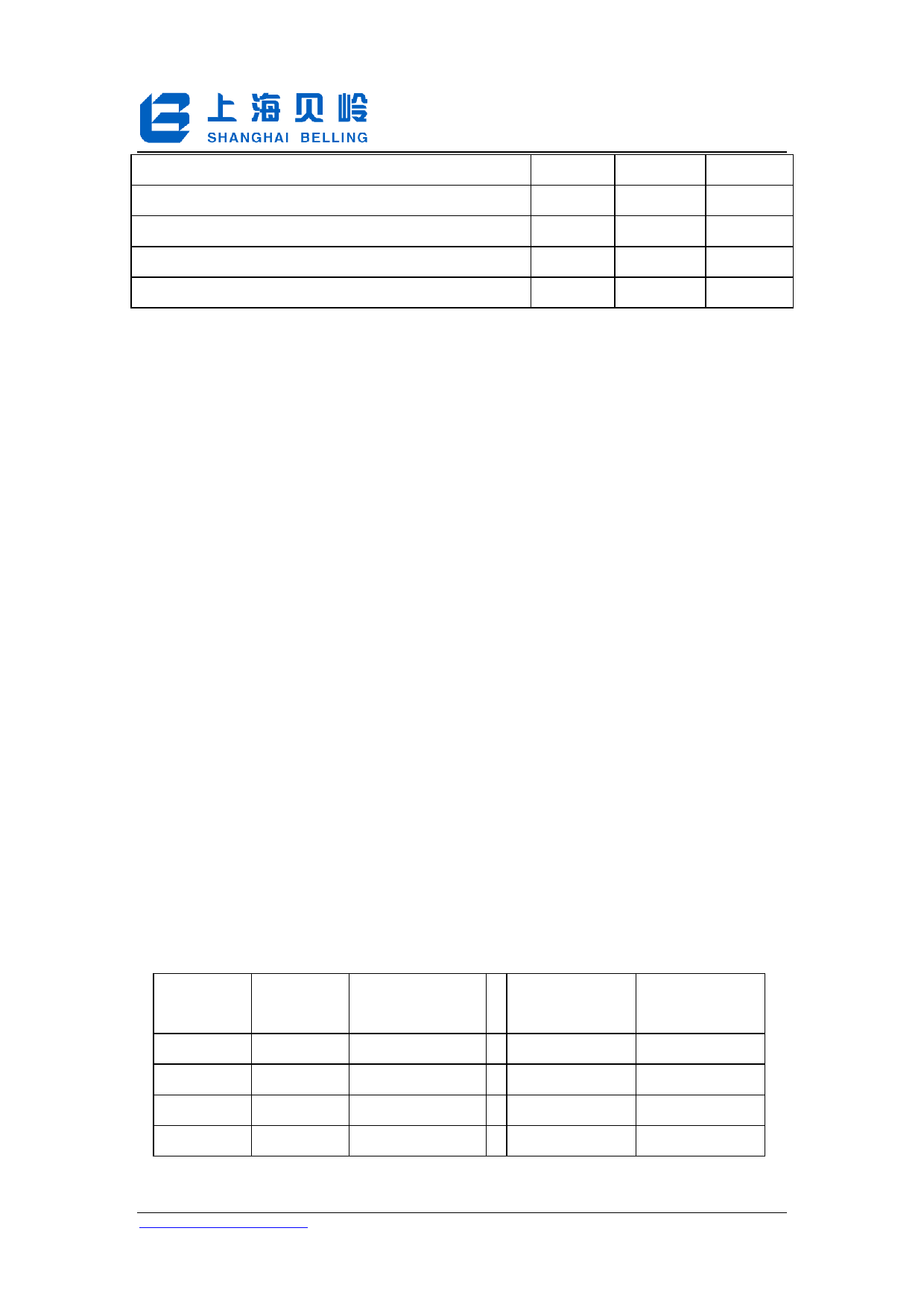
three inputs. The relationship of the inputs and ouput is summarized in the following truth table:
Tx – Rx Transmit Volume Control
∆Vacf
Mode
Comp
Det Comp
Transmit Transmit
No Effect
6.0 mV
Transmit
Transmit
Idle
No Effect
75 mV
Idle
Receive
Transmit
Affects ∆Vacf
50 – 150 mV
Receive
Receive
Idle
Affects ∆Vacf
50 – 150 mV
Receive
http://www.belling.com.cn
-7-
Total 16 Pages
8/15/2006
Wrote by 2006
Share Link: 