BL3406B-15PTRN 데이터 시트보기 (PDF) - Shanghai Belling Co., Ltd.
부품명
상세내역
제조사
BL3406B-15PTRN Datasheet PDF : 11 Pages
| |||
BL3406B
1.5 MHz, 800mA Synchronous Buck Converter
Pin Description
PIN
NAME
FUNCTION
Regulator Enable Control Input. Drive RUN above 1.5V to turn on the part.
1
RUN Drive RUN below 0.3V to turn it off. In shutdown, all functions are disabled
drawing <1µA supply current. Do not leave RUN floating.
2
GND Ground
Power Switch Output. It is the switch node connection to external inductor. This
3
SW
pin connects to the drains of the internal P-Channel and N-Channel MOSFET
switches.
4
VIN
Supply Input Pin. Must be closely decoupled to GND, Pin 2, with a 2.2µF or
greater ceramic capacitor.
VFB (BL3406B-Adj): Feedback Input Pin. Connect FB to the center point of the
external resistor divider. The regulated voltage on this pin is 0.6V.
5
VFB/VOUT VOUT (BL3406B-1.2/BL3406B-1.5/BL3406B-1.8): Output Voltage Feedback Pin.
An internal resistive divider divides the output voltage down for comparison to the
internal reference voltage.
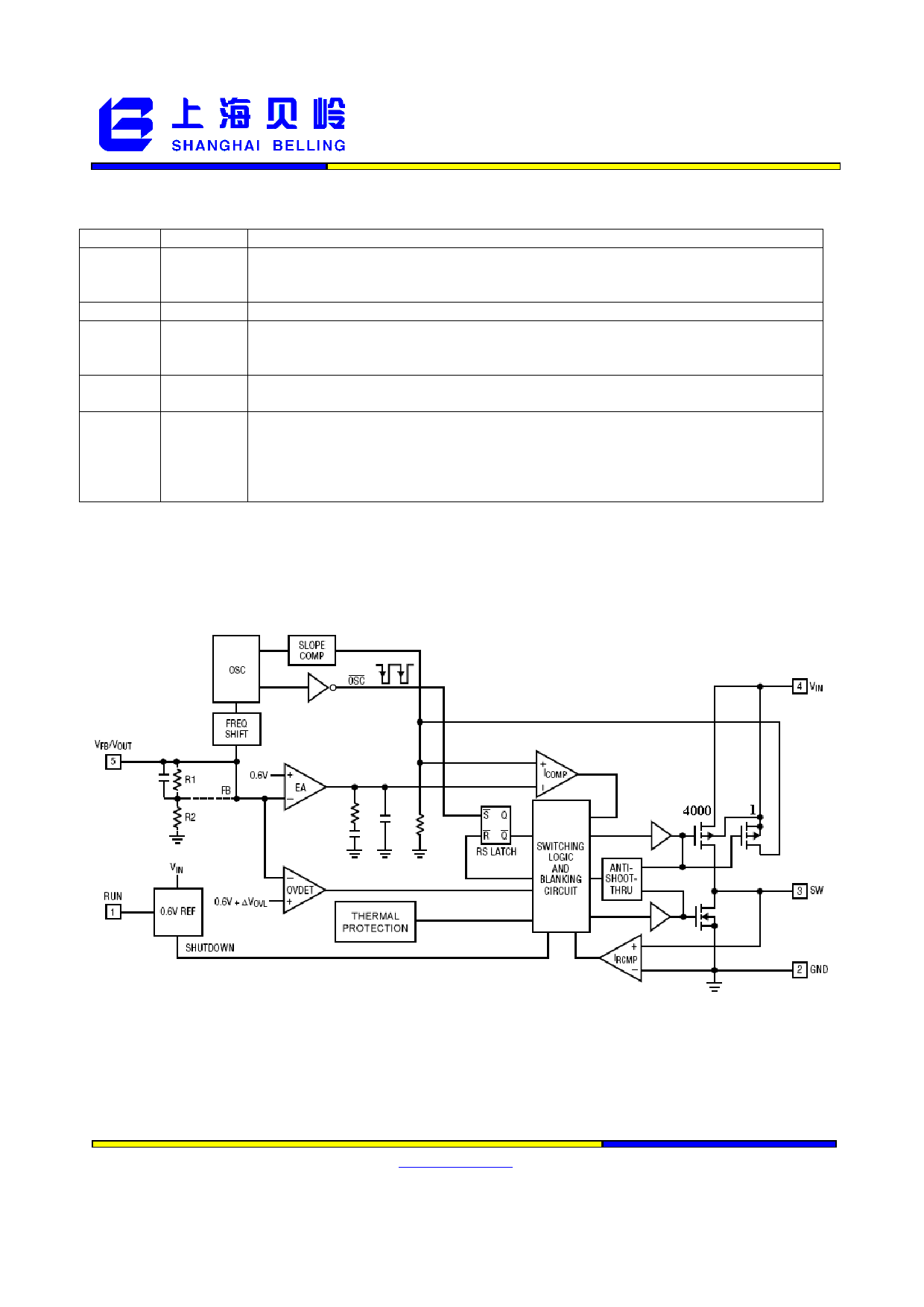
Block Diagram
PPMIC BU
www.belling.com.cn
3
BL3406B Rev 1.5
Belling Proprietary Information. Unauthorized Photocopy and Duplication Prohibited
10/2009
©2009 Belling All Rights Reserved
Share Link: 