BL3406B-15CRN 데이터 시트보기 (PDF) - Shanghai Belling Co., Ltd.
부품명
상세내역
제조사
BL3406B-15CRN Datasheet PDF : 11 Pages
| |||
BL3406B
1.5 MHz, 800mA Synchronous Buck Converter
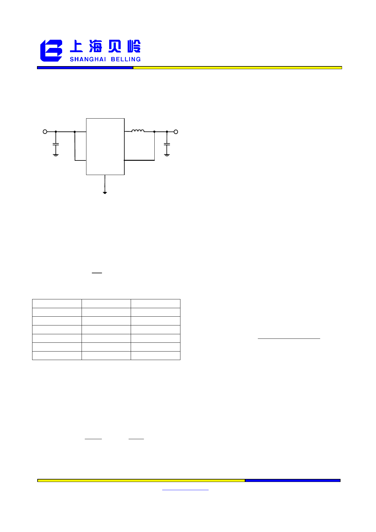
Application Information
Figure 2 below shows the basic application
circuit with BL3406B fixed output versions.
2.7V - 4.2V
VIN
C1
4.7uF
4 VIN
L1
SW 3 2.2µH
BL3406B-18
1 Run
VOUT 5
GND
2
VOUT1.8V
C2
10uF
Figure 2. Basic Application Circuit
with fixed output versions
Setting the Output Voltage
Figure 1 above shows the basic application
circuit with BL3406B adjustable output
version. The external resistor sets the output
voltage according to the following equation:
VOUT
= 0.6V × (1 +
R2)
R1
Table 1—Resistor Selection vs.
Output Voltage Setting
VOUT
R1
R2
1.0V
180 kΩ(1%) 120 kΩ(1%)
1.2V
180 kΩ(1%) 180 kΩ(1%)
1.5V
180 kΩ(1%) 270 kΩ(1%)
1.8V
180 kΩ(1%) 360 kΩ(1%)
2.5V
158 kΩ(1%) 499 kΩ(1%)
3.3V
180 kΩ(1%) 810 kΩ(1%)
Inductor Selection
The output inductor is selected to limit the
ripple current to some predetermined value,
typically 20%~40% of the full load current at
the maximum input voltage. In continuous
mode, the ripple current is determined by:
∆I L =
f
1
×
L VOUT
(1− VOUT
VIN
)
A reasonable starting point for setting ripple
current is ∆IL=320mA (40% of 800mA). For
output voltages above 2.0V, when efficiency
at light load condition is important, the
minimum recommended inductor is 2.2µH.
For optimum voltage-positioning load
transients, choose an inductor with DC series
resistance below 150mΩ. For higher
efficiency at heavy loads (above 200mA), or
minimal load regulation (but some transient
overshoot), the resistance should be kept
below 100mΩ. The DC current rating of the
inductor should be at least equal to the
maximum load current plus half the ripple
current to prevent core saturation. Thus, a
1120mA rated inductor should be enough for
most applications (800mA+320mA).
Input Capacitor Selection
The input capacitor reduces the surge current
drawn from the input and switching noise
from the device. The input capacitor
impedance at the switching frequency shall
be less than input source impedance to
prevent high frequency switching current
passing to the input. In continuous mode, the
source current of the main switch is a square
wave of duty cycle VOUT/VIN. To prevent large
voltage transients, a low ESR input capacitor
sized for the maximum RMS current must be
used. The maximum RMS capacitor current is
given by:
I RMS
≈
I OMAX
[VOUT (VIN −VOUT )]0.5
VIN
This formula has a maximum at VIN =2VOUT,
where IRMS = IOUT/2. This simple worst-case
condition is commonly used for design
because even significant deviations do not
offer much relief. Ceramic capacitors with
X5R or X7R dielectrics are recommended
due to their low ESR and high ripple current.
Output Capacitor Selection
The output capacitor is required to keep the
output voltage ripple small and to ensure
regulation loop stability. The output capacitor
must have low impedance at the switching
PPMIC BU
www.belling.com.cn
8
BL3406B Rev 1.5
Belling Proprietary Information. Unauthorized Photocopy and Duplication Prohibited
10/2009
©2009 Belling All Rights Reserved
Share Link: 