BS616UV4016ECG10 데이터 시트보기 (PDF) - Brilliance Semiconductor
부품명
상세내역
제조사
BS616UV4016ECG10 Datasheet PDF : 10 Pages
| |||
BSI
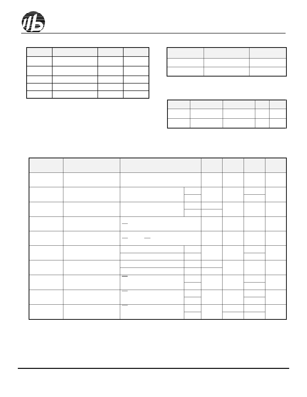
n ABSOLUTE MAXIMUM RATINGS (1)
SYMBOL
VTERM
TBIAS
TSTG
PT
IOUT
PARAMETER
Terminal Voltage with
Respect to GND
Temperature Under
Bias
Storage Temperature
Power Dissipation
DC Output Current
RATING
-0.5(2) to 4.6V
-40 to +85
-60 to +150
1.0
20
UNITS
V
OC
OC
W
MA
1. Stresses greater than those listed under ABSOLUTE MAXIMUM
RATINGS may cause permanent damage to the device. This is a
stress rating only and functional operation of the device at these
or any other conditions above those indicated in the operational
sections of this specification is not implied. Exposure to absolute
maximum rating conditions for extended periods may affect
reliability.
2. –2.0V in case of AC pulse width less than 30 ns
BS616UV4016
n OPERATING RANGE
RANG
Commercial
Industrial
AMBIENT
TEMPERATURE
0OC to + 70OC
-40OC to + 85OC
Vcc
1.8V ~ 3.6V
1.9V ~ 3.6V
n CAPACITANCE (1) (TA = 25OC, f = 1.0MHz)
SYMBOL PAMAMETER CONDITIONS MAX. UNITS
CIN
Input
Capacitance
CIO
Input/Output
Capacitance
VIN = 0V
VI/O = 0V
6
pF
8
pF
1. This parameter is guaranteed and not 100% tested.
n DC ELECTRICAL CHARACTERISTICS (TA = -40OC to +85OC)
PARAMETER
NAME
PARAMETER
TEST CONDITIONS
MIN. TYP.(1) MAX. UNITS
VCC
Power Supply
1.9
--
3.6
V
VIL
Input Low Voltage
VIH
Input High Voltage
IIL
ILO
VOL
VOH
ICC
ICCSB
ICCSB1(5)
Input Leakage Current
VIN = 0V to VCC,
CE = VIH
Output Leakage Current
VI/O = 0V to VCC
CE= VIH, or OE = VIH
Output Low Voltage
Output High Voltage
Operating Power
Current
Supply
VCC = Max, IOL = 0.1mA
VCC = Max, IOL = 2.0mA
VCC = Min, IOH = -0.1mA
VCC = Min, IOH = -1.0mA
CE = VIL,
IIO = 0mA, f = FMAX(4)
Standby Current – TTL
CE = VIH,
IIO = 0mA
Standby Current – CMOS
CE≧VCC-0.2V,
VIN≧VCC-0.2V or VIN≦0.2V
1. Typical characteristics are at TA=25OC.
2. Undershoot: -1.0V in case of pulse width less than 20 ns.
3. Overshoot: VCC+1.0V in case of pulse width less than 20 ns.
4. FMAX=1/tRC.
5. ICCSB1(MAX) is 3.0/6.0uA at VCC=2.0V/3.0V and TA=70OC.
VCC=2.0V
VCC=3.0V
VCC=2.0V
VCC=3.0V
-0.3(2)
1.4
2.0
--
0.6
--
V
0.8
--
VCC+0.3(3)
V
--
1
uA
--
--
1
uA
VCC=2.0V
--
VCC=3.0V
0.2
--
V
0.4
VCC=2.0V VCC-0.2
--
--
V
VCC=3.0V
2.4
VCC=2.0V
--
VCC=3.0V
12
--
mA
15
VCC=2.0V
--
VCC=3.0V
0.5
--
mA
1.0
VCC=2.0V
--
0.3
5.0
uA
VCC=3.0V
0.45
8.0
R0201-BS616UV4016
3
Revision 1.3
Sep. 2005
Share Link: 