PDM34089SA10QTR 데이터 시트보기 (PDF) - Paradigm Technology
부품명
상세내역
제조사
PDM34089SA10QTR Datasheet PDF : 15 Pages
| |||

PRELIMINARY
PDM34089
Burst Mode Operation
This is a synchronous part. All activities are initiated by the positive, low-to-high edge of the clock (CLK). This part can
perform burst reads and writes with burst lengths of up to four words. The four-word burst is created by using a burst
counter to drive the two least-significant bits of the internal RAM address. The burst counter is loaded at the start of the
burst and is incremented for each word of the burst. The sequence is given in the Burst Sequence Table.
Burst transfers are initiated by the ADSC or ADSP signals. When the ADSP and CE signals are sampled low, a read cycle
is started (independent of BW1, BW2, BW3 or BW4; BWE, GW and ADSC), and prior burst activity is terminated. ADSP
is gated by CE, so both must be active for ADSP to load the address register and to initiate a read cycle. The address and
the chip enable input (CE) are sampled by the same edge that samples ADSP. Read data is valid at the output after the
specified delay from the clock edge.
When ADSC is sampled low and ADSP is sampled high, a read or write cycle is started depending on the state of BW1,
BW2, BW3 or BW4; BWE, and GW. If BW1, BW2, BW3, BW4, BWE, and GW are all sampled high, a read cycle is started,
as described above. If BW1, BW2, BW3, or BW4; BWE, and GW is sampled low, a write cycle is begun. The address,
write data, and the chip enable inputs (CE, CE2 and CE2) are sampled by the same edge that samples ADSC and BW1–
BW4, BWE and GW. The ADV line is held high for this clock edge to maintain the correct address for the internal write
operation which will follow this second clock edge.
After the first cycle of the write burst, the state of BW1-BW4, BWE and GW determines whether the next cycle is a read
or write cycle, and ADV controls the advance of the address counter. The ADV signal advances the address counter.
This increments the address to the next available RAM address. You write the next word in the burst by taking ADV low
and presenting the write data at the positive edge of the clock. If ADV is sampled low, the burst counter advances and
the write data (which is sampled by the same clock) is written into the internal RAM during the time following the clock
edge.
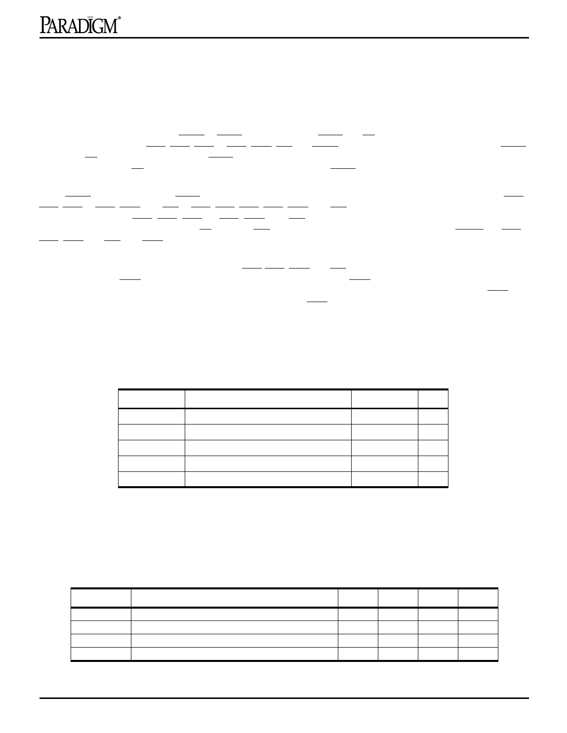
Absolute Maximum Ratings
Symbol
Rating
Com’l.
Unit
VTERM
TA
TBIAS
TSTG
IOUT
Terminal Voltage with Respect to VSS
Operating Temperature
Temperature Under Bias
Storage Temperature
DC Output Current
–0.5 to +4.6
V
0 to +70
°C
–55 to +125
°C
–55 to +125
°C
100
mA
NOTE:
1. Stresses greater than those listed under ABSOLUTE MAXIMUM RATINGS
may cause permanent damage to the device. This is a stress rating only and
functional operation of the device at these or any other conditions above
those indicated in the operational sections of this specification is not implied.
Exposure to absolute maximum rating conditions for extended periods may
affect reliability.
Recommended DC Operating Conditions
Symbol
Description
VCC
VCCQ
VSS
Commercial
Supply Voltage
Supply voltage
Supply Voltage
Ambient Temperature
Min.
Typ.
Max.
Unit
3.1
3.3
3.6
V
3.1
3.3
3.6
V
0
0
0
V
0
25
70
°C
6
Rev 1.1 - 5/01/98