IDT74FCT163543 데이터 시트보기 (PDF) - Integrated Device Technology
부품명
상세내역
제조사
IDT74FCT163543 Datasheet PDF : 7 Pages
| |||
IDT74FCT163543/A/C
3.3V CMOS 16-BIT LATCHED TRANSCEIVER
COMMERCIAL TEMPERATURE RANGE
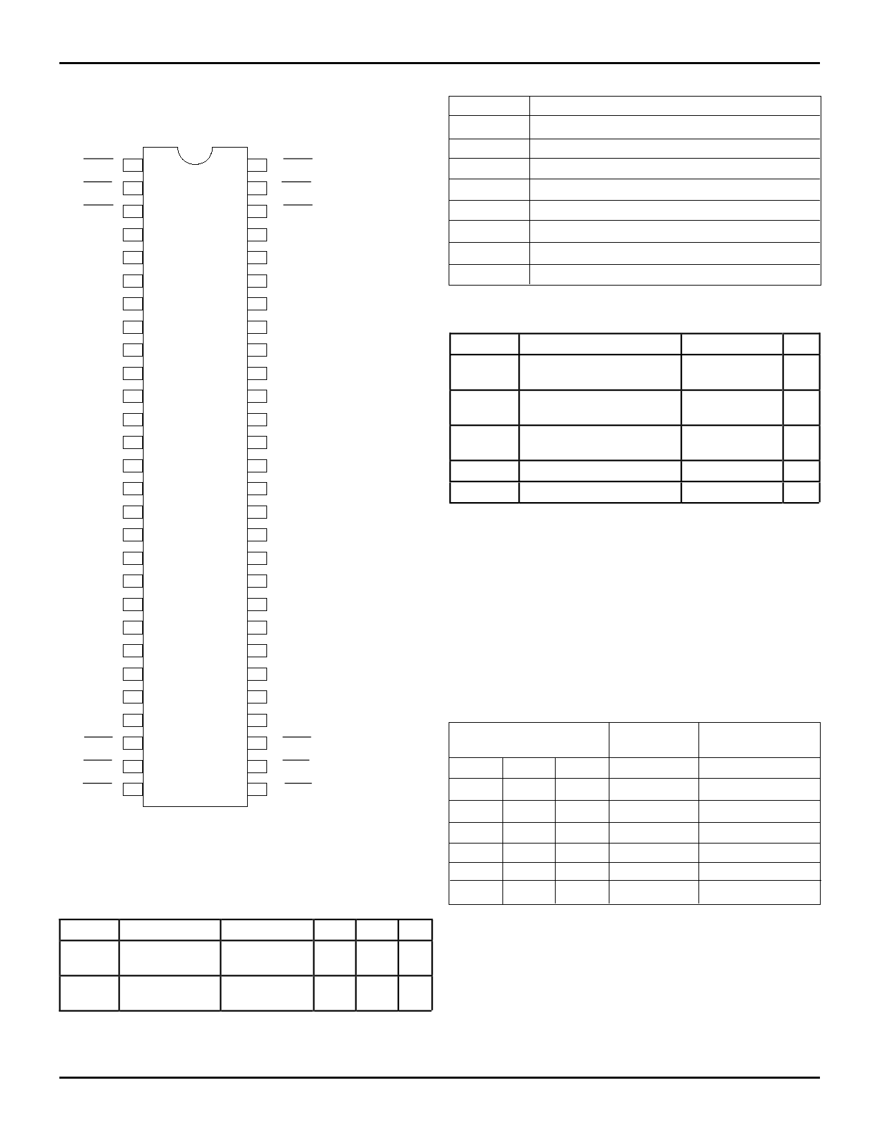
PIN CONFIGURATIONS
1OEAB
1LEAB
1CEAB
GND
1A1
1A2
VCC
1A3
1A4
1A5
GND
1A6
1A7
1A8
2A1
2A2
2A3
GND
2A4
2A5
2A6
VCC
2A7
2A8
GND
2CEAB
2LEAB
2OEAB
1
56
2
55
3
54
4
53
5
52
6
51
7
50
8
49
9
48
10
47
11
46
12
45
13
44
14 SO56-1 43
SO56-2
15 SO56-3 42
16
41
17
40
18
39
19
38
20
37
21
36
22
35
23
34
24
33
25
32
26
31
27
30
28
29
SSOP/
TSSOP/TVSOP
TOP VIEW
1OEBA
1LEBA
1CEBA
GND
1B1
1B2
VCC
1B3
1B4
1B5
GND
1B6
1B7
1B8
2B1
2B2
2B3
GND
2B4
2B5
2B6
VCC
2B7
2B8
GND
2CEBA
2LEBA
2OEBA
3250 drw 03
CAPACITANCE (TA = +25°C, f = 1.0MHz)
Symbol Parameter(1) Conditions Typ. Max. Unit
CIN
Input
VIN = 0V
3.5 6.0 pF
Capacitance
CI/O
I/O
VOUT = 0V 3.5 8.0 pF
Capacitance
NOTE:
3250 lnk 04
1. This parameter is measured at characterization but not tested.
PIN DESCRIPTION
Pin Names
xOEAB
xOEBA
xCEAB
xCEBA
xLEAB
xLEBA
Description
A-to-B Output Enable Input (Active LOW)
B-to-A Output Enable Input (Active LOW)
A-to-B Enable Input (Active LOW)
B-to-A Enable Input (Active LOW)
A-to-B Latch Enable Input (Active LOW)
B-to-A Latch Enable Input (Active LOW)
xAx
A-to-B Data Inputs or B-to-A 3-State Outputs
xBx
B-to-A Data Inputs or A-to-B 3-State Outputs
3250 tbl 01
ABSOLUTE MAXIMUM RATINGS(1)
Symbol
VTERM(2)
VTERM(3)
VTERM(4)
TSTG
Description
Terminal Voltage with
Respect to GND
Terminal Voltage with
Respect to GND
Terminal Voltage with
Respect to GND
Storage Temperature
Max.
Unit
–0.5 to +4.6 V
–0.5 to +7.0 V
–0.5 to
V
VCC + 0.5
–65 to +150 °C
IOUT
DC Output Current
–60 to +60 mA
NOTES:
3250 lnk 03
1. Stresses greater than those listed under ABSOLUTE MAXIMUM RAT-
INGS may cause permanent damage to the device. This is a stress rating
only and functional operation of the device at these or any other conditions
above those indicated in the operational sections of this specification is
not implied. Exposure to absolute maximum rating conditions for ex-
tended periods may affect reliability.
2. Vcc terminals.
3. Input terminals.
4. Output and I/O terminals.
FUNCTION TABLE(1, 3)
For A-to-B (Symmetric with B-to-A)
Inputs
xCEAB xLEAB xOEAB
Latch
Status
xAx to xBx
H
X
X
Storing
X
H
X
Storing
L
L
L
Transparent
L
H
L
Storing
L
L
H
Transparent
L
H
H
Storing
Output
Buffers
xBx
High Z
X
Current A Inputs
Previous(2) A Inputs
High Z
High Z
NOTES:
3250 tbl 02
1. A-to-B data flow shown; B-to-A flow control is the same, except using
xCEBA, x LEBA and xOEBA.
2. Before xLEAB LOW-to-HIGH Transition
3. H = HIGH Voltage Level
L = LOW Voltage Level
X = Don’t Care
8.7
2
Share Link: 