MAX729 데이터 시트보기 (PDF) - Maxim Integrated
부품명
상세내역
제조사
MAX729 Datasheet PDF : 4 Pages
| |||
5V/3.3V/3V 2A Step-Down, PWM,
Switch-Mode DC-DC Regulators
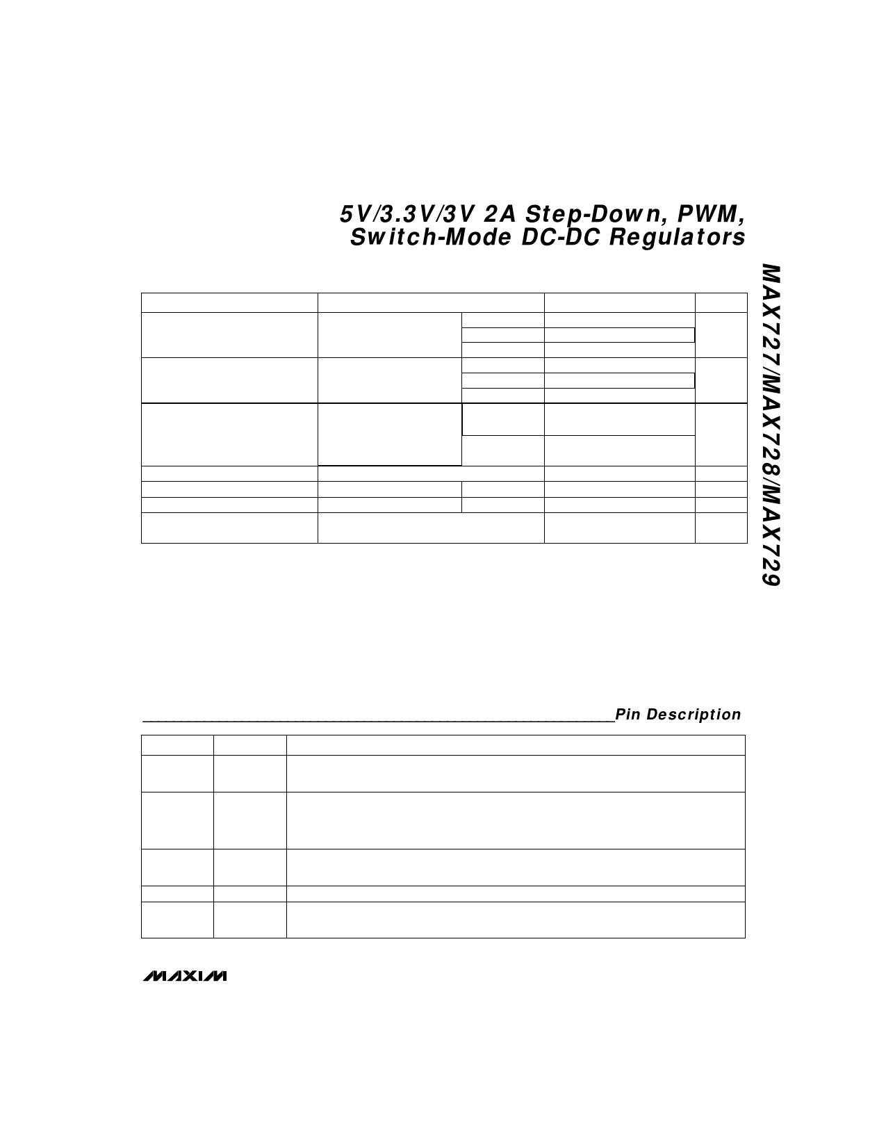
ELECTRICAL CHARACTERISTICS (continued)
(VIN = 25V, Tj = TMIN to TMAX, unless otherwise noted.)
PARAMETER
CONDITIONS
MIN
MAX727
4.85
SENSE Voltage
VC = 2V
MAX728
3.20
MAX729
2.90
MAX727
3.0
SENSE Pin Divider Resistance
Tj = +25°C
MAX728
2.5
MAX729
2.2
Output Voltage Tolerance
VOUT (nominal) = 5V (MAX727),
3.3V (MAX728), or 3V (MAX729); Tj = +25°C
all conditions of input voltage,
output voltage, and load
Tj = TMIN to
current
TMAX
Output Voltage Line Regulation
8V ≤ VIN ≤ 40V
VC Voltage
0% duty cycle
Tj = +25°C
VC Voltage Temperature Coefficient 0% duty cycle
Tj = TMIN to TMAX
Thermal Resistance Junction to Case
(Note 6)
TYP
5.00
3.30
3.00
5.0
4.2
3.8
±0.5
MAX
5.15
3.40
3.10
8.0
7.0
6.5
±2.0
±1.0
0.005
1.5
-4
±3.0
0.020
4.0
UNITS
V
kΩ
%
%/V
V
mV/°C
°C/W
Note 1: Do not exceed switch-to-input voltage limitation.
Note 2: For switch currents between 1A and 2A, maximum switch-on voltage can be calculated via linear interpolation.
Note 3: By setting the SENSE pin to 5.5V, the VC pin is forced to its low clamp level and the switch duty cycle is forced to zero,
approximating the zero load condition.
Note 4: For proper regulation, total voltage from VIN to GND must be ≥ 8V after start-up.
Note 5: To avoid extremely short switch-on times, the switch frequency is internally scaled down when VSENSE is less than 2.6V
(MAX727), 2.0V (MAX728), or 1.8V (MAX729). Switch current limit is tested with VSENSE adjusted to give a 1µs minimum
switch-on time.
Note 6: Guaranteed, not production tested.
______________________________________________________________Pin Description
PIN
NAME
FUNCTION
1
SENSE
SENSE Input is the internal error amplifier's input, and should be directly connected to VOUT.
SENSE also aids current limiting by reducing oscillator frequency when VOUT is low.
Error-Amplifier Output. A series RC network connected to this pin compensates the
2
VC
MAX727/MAX728/MAX729. Output swing is limited to about 5.8V in the positive direction and
-0.7V in the negative direction. VC can also synchronize the MAX727/MAX728/MAX729 to an
external TTL clock in the 115kHz to 170kHz range. See MAX724/MAX726 data sheet.
3
GND
Ground requires a short, low-noise connection to ensure good load regulation. The internal refer-
ence is referred to GND, so errors at this pin are multiplied by the error amplifier.
4
VSW
Internal Power Switch Output. The Switch output can swing 35V below ground and is rated for 2A.
5
VIN
VIN supplies power to the internal circuitry and also connects to the collector of the internal power
switch. VIN must be bypassed with a low-ESR capacitor, typically 200µF or 220µF.
_______________________________________________________________________________________ 3
Share Link: 