PI6C39911J 데이터 시트보기 (PDF) - Pericom Semiconductor Corporation
부품명
상세내역
제조사
PI6C39911J
Pericom Semiconductor Corporation

PI6C39911J Datasheet PDF : 11 Pages
| |||
PI6C39911/PI6C39912
3.3V High Speed LVTTL or Balanced Output
11223344556677889900112233445566778899001122334455667788990011221122334455667788990011223344556677889900112233445566778899001122112233445566778899001122P3344r5566o77g8899r00a1122m3344m556677a88b9900l11e2211S2233k44e5566w7788C990011l22o33c44k556677B8899u0011f22f33e44r5566-7788S99u0011p2211e22r33C4455l66o7788c99k0011®22
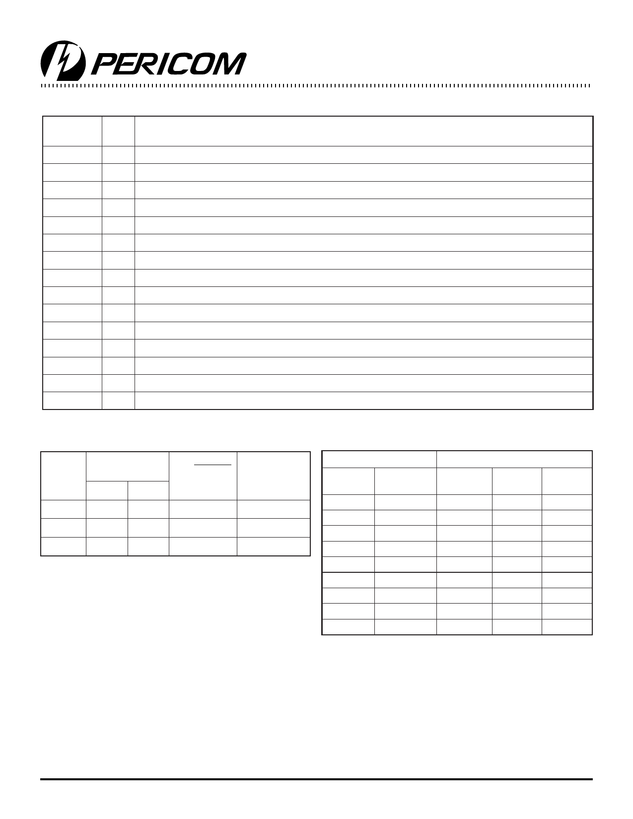
Pin Descriptions
Signal
Name
I/O
Description
REF
I Reference frequency input supplies the frequency and timing against which all functional variation is measured.
FB
I PLL feedback input (typically connected to one of the eight outputs)
FS
I Three-level frequency range select. see Table 1.
1F0, 1F1 I Three-level function select inputs for output pair 1 (1Q0, 1Q1). see Table 2.
2F0, 2F1 I Three-level function select inputs for output pair 2 (2Q0, 2Q1). see Table 2.
3F0, 3F1 I Three-level function select inputs for output pair 3 (3Q0, 3Q1). see Table 2.
4F0, 4F1 I Three-level function select inputs for output pair 4 (4Q0, 4Q1). see Table 2.
TEST
I Three-level select. See test mode section under the block diagram descriptions
1Q0, 1Q1 O Output pair 1. see Table 2
2Q0, 2Q1 O Output pair 2. see Table 2
3Q0, 3Q1 O Output pair 3. see Table 2
4Q0, 4Q1 O Output pair 4. see Table 2
VCCN PWR Power supply for output drivers
VCCQ PWR Power supply for internal circuitry
GND PWR Ground
Table 1. Frequency Range Select and tU Calculation(1)
Table 2. Programmable Skew Configurations(1)
FS(1,2)
LOW
MID
HIGH
FNOM (MHz)
Min.
12.5
25
40
Max.
30
50
133
tU =
1
fNOM × N
where N=
Approximate
Freq. (MHz) at
which tU= 1.0ns
44
22.7
26
38.5
16
62.5
Function Selects
1F1, 2F1,
3F1, 4F1
1F0, 2F0,
3F0, 4F0
LOW
LOW
LOW
MID
LOW
HIGH
MID
LOW
Output Functions
1Q0, 1Q1,
2Q0, 2Q1
3Q0, 3Q1
4Q0, 4Q1
4tU Divide by 2 Divide by 2
3tU
6tU
6tU
2tU
4tU
4tU
1tU
2tU
2tU
MID
MID
0tU
0tU
0tU
MID
HIGH
+1tU
+2tU
+2tU
HIGH
LOW
+2tU
+4tU
+4tU
HIGH
MID
+3tU
+6tU
+6tU
HIGH
HIGH
+4tU Divide by 4 Inverted
Notes:
1. For all three-state inputs, HIGH indicates a connection to VCC, LOW indicates a connection to GND, and MID indicates an open
connection. Internal termination circuitry holds an unconnected input to VCC/2.
2. The level to be set on FS is determined by the normal operating frequency (fNOM) and Time Unit Generator (see Logic Block Diagram).
Nominal frequency (fNOM) always appears at 1Q0 and the other outputs when they are operated in their undivided modes (see Table
2). The frequency appearing at the REF and FB inputs will be f NOM when the output connected to FB is undivided. The frequency
of the REF and FB inputs will be fNOM/2 or fNOM/4 when the part is configured for a frequency multiplication by using a divided output
as the FB input.
2
PS8497A 04/10/01
Share Link: