RMPA0913C-58 데이터 시트보기 (PDF) - Raytheon Company
부품명
상세내역
제조사
RMPA0913C-58 Datasheet PDF : 6 Pages
| |||
RMPA0913C-58
3.5V AMPS/CDMA Power Amplifier
Test Procedure
for the evaluation board
(RMPA0913C-58)
PRODUCT INFORMATION
CAUTION: LOSS OF GATE VOLTAGES (VG1, VG2) WHILE DRAIN VOLTAGES (VD1,VD2) ARE PRESENT MAY
DAMAGE THE AMPLIFIER.
The following sequence must be followed to properly test the amplifier:
Step 1: Turn off RF input power.
Step 2: Use GND terminal of the evaluation board for
the ground of the DC supplies. Slowly apply
gate supply voltages of -3.0 V to the board
terminals Vgg1, Vgg2 to pinch-off the two
stages.
Step 3: Slowly apply drain supply voltage of +3.5 V to
the board terminals Vdd.
Step 4: Adjust the gate supply voltages Vgg1, Vgg2 to
the values shown on the data summary supplied
with the sample. (First adjust Vgg2 to set Idq2.
Then adjust Vgg1 to set Iddq=Idq1+Idq2. These
gate voltages need not be changed. However,
Vgg1,Vgg2 may be adjusted only when different
quiescent bias currents are desired for
performance trade-off evaluation).
Step 5: After the bias condition is established, RF input
signal may now be applied at the appropriate
frequency band. Adjust RF input signal power
level as required.
Step 6: Follow turn-off sequence of:
(i) Turn off RF Input Power
(ii) Turn down and off drain voltage Vdd.
(iii) Turn down and off gate voltages Vgg1, Vgg2.
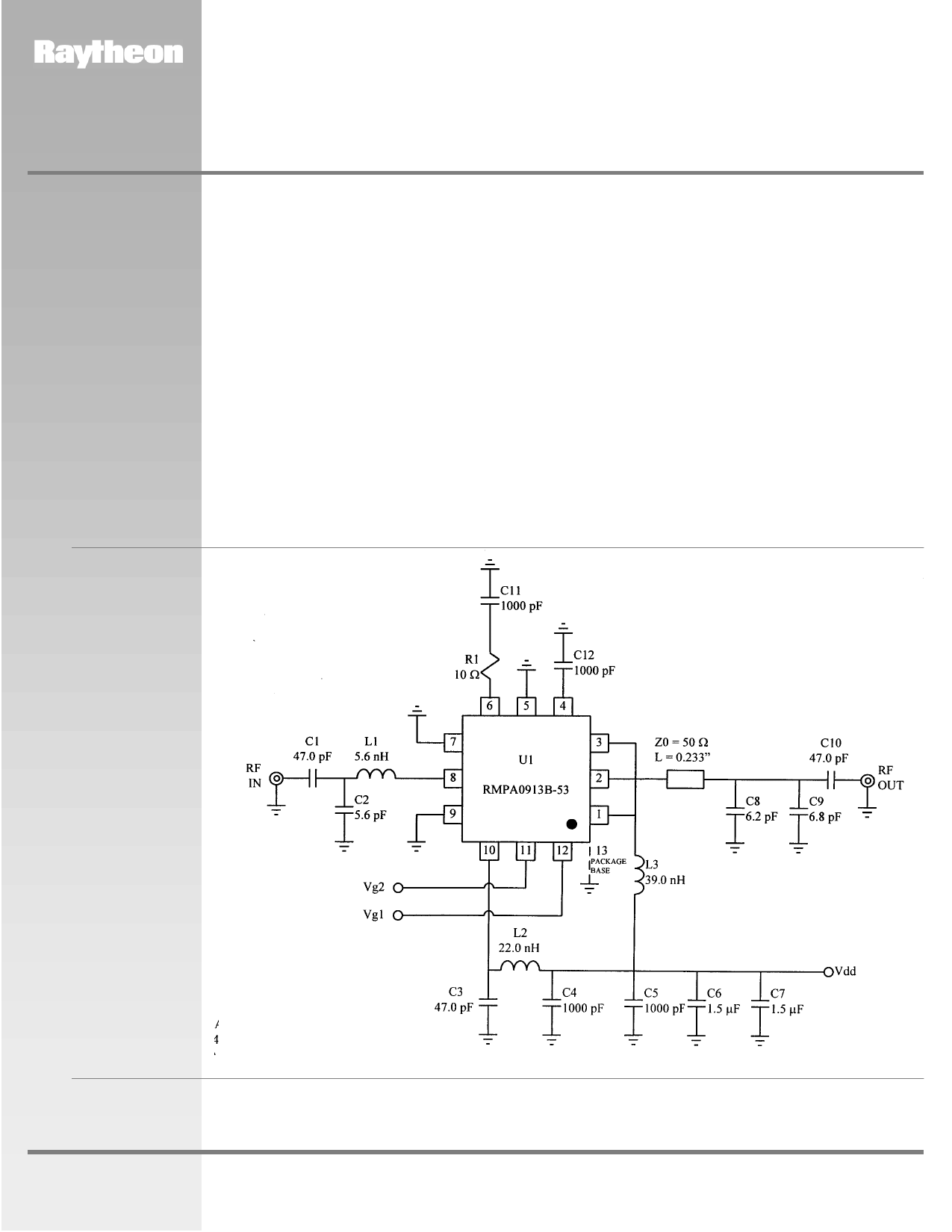
Figure 3
Schematic
for a Typical Test
Evaluation Board
Evaluation Board Schematic
Ver.6, 4/28/98
Board Type: Multi Layer FR4
Signal to Ground Separation: 0.016”
www.raytheon.com/micro
Characteristic performance data and specifications are subject to change without notice.
Revised March 30, 2000
Page 3
Raytheon RF Components
362 Lowell Street
Andover, MA 01810
Share Link: 