CA5130 데이터 시트보기 (PDF) - Intersil
부품명
상세내역
제조사
CA5130 Datasheet PDF : 19 Pages
| |||
CA5130, CA5130A
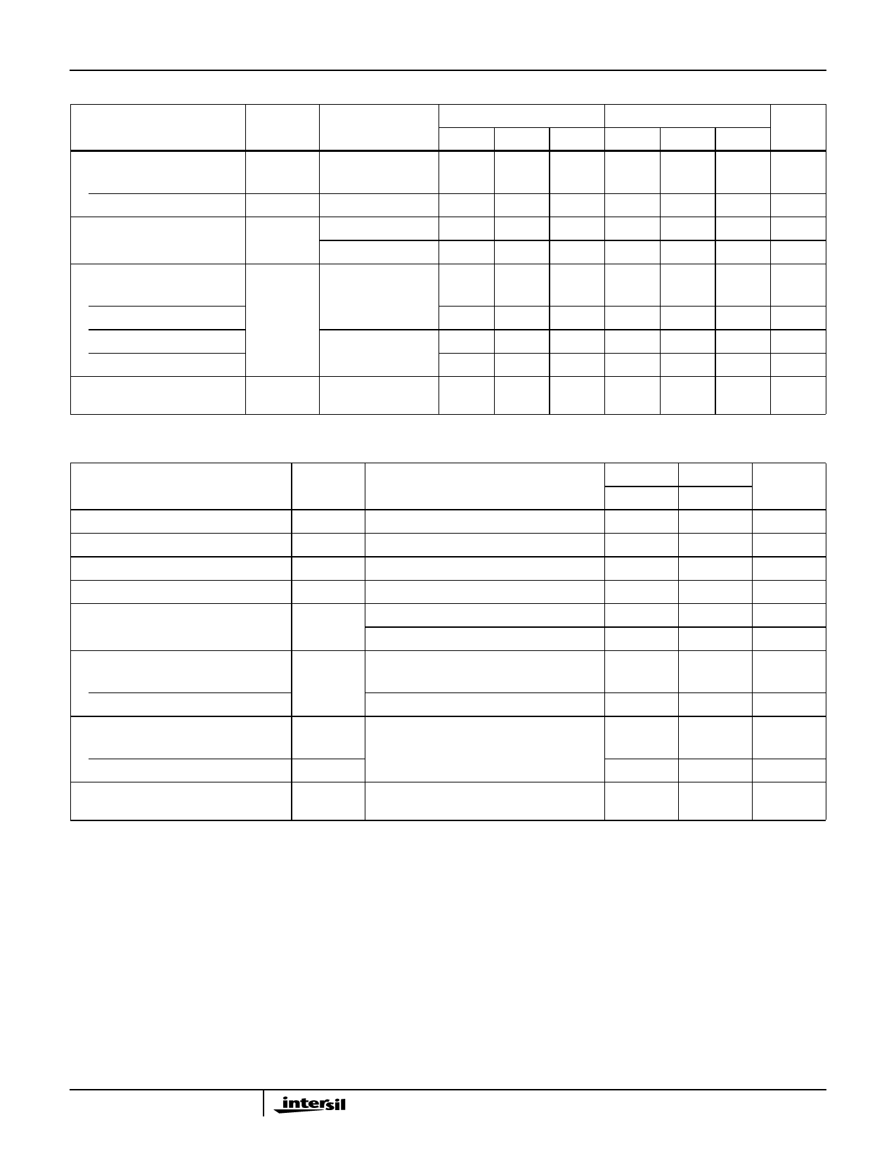
Electrical Specifications
PARAMETER
Maximum Output Current
Source
Sink
Supply Current
Maximum Output Voltage
VOM+
VOM-
VOM+
VOM-
Input Offset Voltage
Temperature Drift
TA = 25oC, V+ = 15V, V- = 0V, Unless Otherwise Specified (Continued)
SYMBOL
TEST
CONDITIONS
CA5130
MIN
TYP
MAX
MIN
CA5130A
TYP
MAX
UNITS
IOM+ VO = 0V
12
22
45
12
22
45
mA
IOM-
VO = 15V
12
20
45
12
20
45
mA
ISUPPLY VO = 7.5V, RL = ∞
-
10
15
-
10
15
mA
VO = 0V, RL = ∞
-
2
3
-
2
3
mA
VOUT
RL = ∞
14.99
15
-
14.99
15
-
V
-
0
0.01
-
0
0.01
V
RL = 2kΩ
∆VIO/∆T
12
13.3
-
-
0.002 0.01
-
10
-
12
13.3
-
V
-
0.002 0.01
V
-
10
-
µV/oC
Electrical Specifications
Typical Values Intended Only for Design Guidance, At TA = 25oC, VSUPPLY = ±7.5V
Unless Otherwise Specified
CA5130 CA5130A
PARAMETER
SYMBOL
TEST CONDITIONS
TYP
TYP
Input Offset Voltage Adjustment Range
10kΩ Across Terminals 4 and 5 or 4 and 1
±22
±22
Input Resistance
Input Capacitance
Equivalent Input Noise Voltage
Open Loop Crossover Frequency
For Unity Gain Stability ≥47pF Required
Slew Rate
Open Loop
Closed Loop
Transient Response
Rise Time
Overshoot
RI
CI
f = 1MHz
eN
BW = 0.2MHz, RS = 1MΩ (Note 5)
fT
CC = 0
CC = 47pF
SR
CC = 0
CC = 56pF
CC = 56pF, CL = 25pF, RL = 2kΩ
tr
(Voltage Follower)
OS
1.5
1.5
4.3
4.3
23
23
15
15
4
4
30
30
10
10
0.09
0.09
10
10
Settling Time (To <0.1%, VIN = 4VP-P)
tS
CC = 56pF, CL = 25pF, RL = 2kΩ
(Voltage Follower)
1.2
1.2
NOTE:
5. Although a 1MΩ source is used for this test, the equivalent input noise remains constant for values of RS up to 10MΩ.
UNITS
mV
TΩ
pF
µV
MHz
MHz
V/µs
V/µs
µs
%
µs
4
Share Link: 