CAT24C208 데이터 시트보기 (PDF) - Catalyst Semiconductor => Onsemi
부품명
상세내역
제조사
CAT24C208 Datasheet PDF : 13 Pages
| |||
CAT24C208
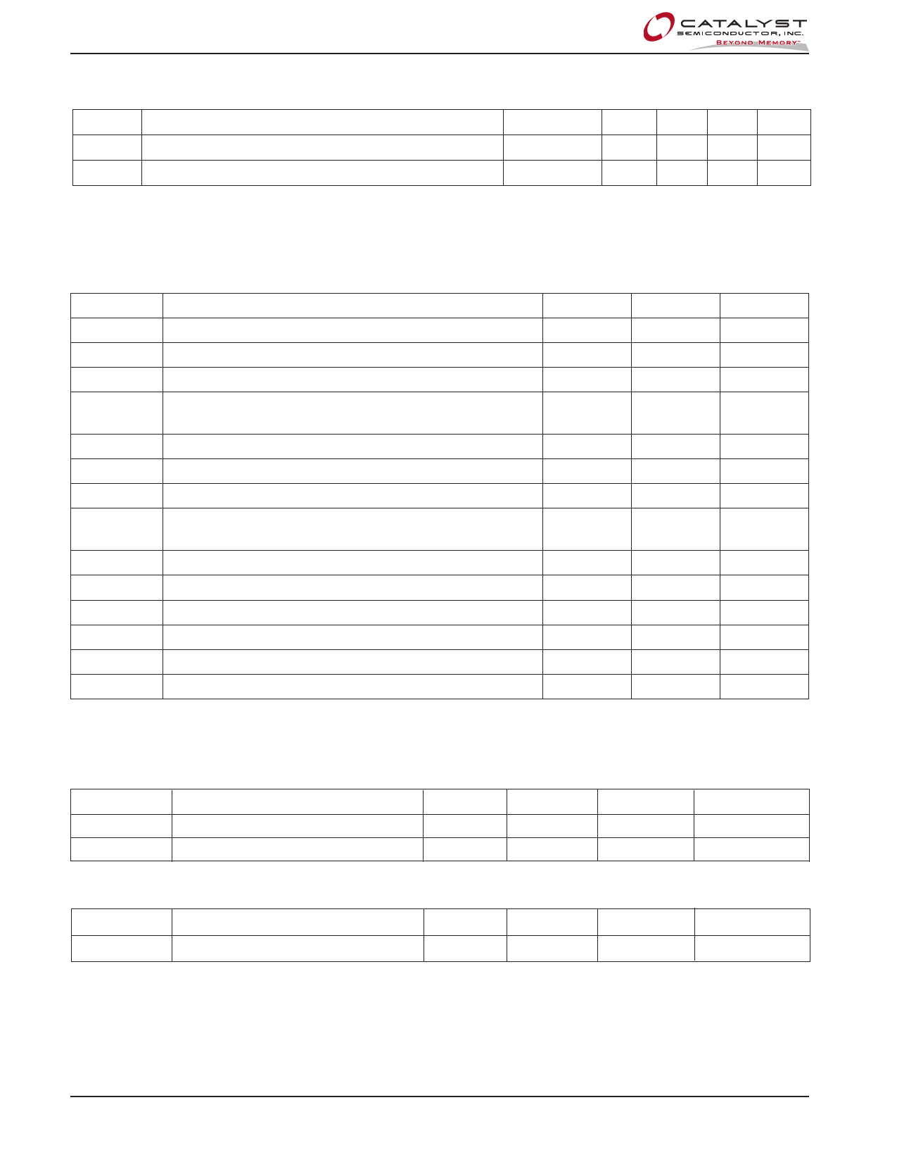
CAPACITANCE TA = 25°C, f = 1.0 MHz, VCC = 5V
Symbol Parameter
Conditions Min Typ
CI/O(1)
CIN(1)
Input/Output Capacitance (Either DSP or DDC SDA) VI/O = 0V
Input Capacitance (EDID, Either DSP or DDC SCL) VIN = 0V
Note:
(1) This parameter is tested initially and after a design or process change that affects the parameter.
A.C. CHARACTERISTICS
VCC = 2.5V to 5.5V, unless otherwise specified.
Read & Write Cycle Limits
Symbol Parameter
Min
Max
FSCL
Clock Frequency
400
TI(1)
Noise Suppression Time Constant at SCL, SDA Inputs
100
tAA
SCL Low to SDA Data Out and ACK Out
0.9
tBUF(1)
Time the Bus Must be Free Before a New Transmission
Can Start
1.3
tHD:STA Start Condition Hold Time
0.6
tLOW
Clock Low Period
1.3
tHIGH
Clock High Period
0.6
tSU:STA
Start Condition Setup Time (for a Repeated Start
Condition)
0.6
tHD:DAT Data In Hold Time
0
tSU:DAT Data In Setup Time
100
tR(1)
SDA and SCL Rise Time
300
tF(1)
SDA and SCL Fall Time
300
tSU:STO Stop Condition Setup Time
0.6
tDH
Data Out Hold Time
100
Note:
(1) This parameter is tested initially and after a design or process change that affects the parameter.
(2) tPUR and tPUW are the delays required from the time VCC is stable until the specified operation can be initiated.
Max Units
8
pF
6
pF
Units
kHz
ns
µs
µs
µs
µs
µs
µs
ns
ns
ns
ns
µs
ns
Power-Up Timing(1)(2)
Symbol
Parameter
Min
Typ
tPUR
tPUW
Power-up to Read Operation
Power-up to Write Operation
Max
Units
1
ms
1
ms
Write Cycle Limits
Symbol
Parameter
Min
Typ
Max
Units
tWR
Write Cycle Time
5
ms
The write cycle time is the time from a valid stop condition of a write sequence to the end of the internal program/erase
cycle. During the write cycle, the bus interface circuits are disabled, SDA is allowed to remain high, and the device does
not respond to its slave address.
Doc. No. 1044, Rev. F
4
© 2006 by Catalyst Semiconductor, Inc.
Characteristics subject to change without notice
Share Link: 