CAT25010 데이터 시트보기 (PDF) - Catalyst Semiconductor => Onsemi
부품명
상세내역
제조사
CAT25010 Datasheet PDF : 17 Pages
| |||
CAT25010, CAT25020, CAT25040
WRITE OPERATIONS
The CAT25010/20/40 device powers up into a write
disable state. The device contains a Write Enable
Latch (WEL) which must be set before attempting to
write to the memory array or to the status register. In
addition, the address of the memory location(s) to be
written must be outside the protected area, as defined
by BP0 and BP1 bits from the status register.
Write Enable and Write Disable
The internal Write Enable Latch and the corresponding
Status Register WEL bit are set by sending the WREN
instruction to the CAT25010/20/40. Care must be taken
to take the C¯¯S input high after the WREN instruction,
as otherwise the Write Enable Latch will not be
properly set. WREN timing is illustrated in Figure 2.
The WREN instruction must be sent prior any WRITE
or WRSR instruction.
The internal write enable latch is reset by sending the
WRDI instruction as shown in Figure 3. Disabling write
operations by resetting the WEL bit, will protect the
device against inadvertent writes.
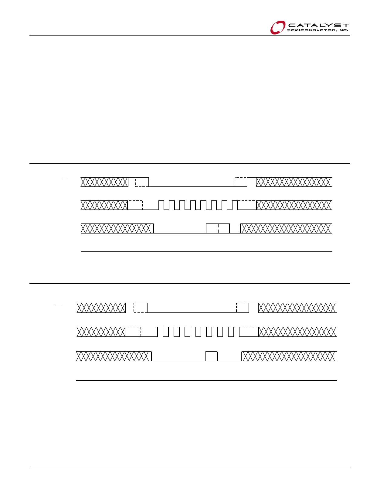
Figure 2. WREN Timing
CS
SCK
SI
SO
Note: Dashed Line = mode (1, 1) - - - - - -
0 0 0 00 1 10
HIGH IMPEDANCE
Figure 3. WRDI Timing
CS
SCK
SI
SO
Note: Dashed Line = mode (1, 1) - - - - - -
0 0 0 0 0 1 00
HIGH IMPEDANCE
Doc. No. MD-1006 Rev. T
6
© Catalyst Semiconductor, Inc.
Characteristics subject to change without notice
Share Link: 