CAT93C66 데이터 시트보기 (PDF) - ON Semiconductor
부품명
상세내역
제조사
CAT93C66 Datasheet PDF : 16 Pages
| |||
CAT93C66, CAT93W66
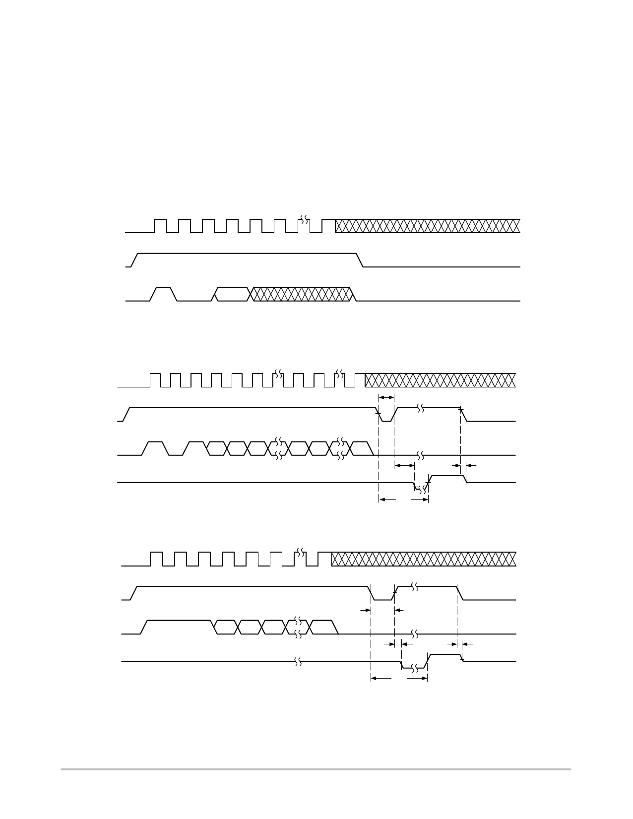
Write
After receiving a WRITE command (Figure 5), address
and the data, the CS (Chip Select) pin must be deselected for
a minimum of tCSMIN. The falling edge of CS will start the
self clocking clear and data store cycle of the memory
location specified in the instruction. The clocking of the SK
pin is not necessary after the device has entered the self
clocking mode. The ready/busy status of the CAT93C66,
CAT93W66 can be determined by selecting the device and
polling the DO pin. Since this device features Auto−Clear
before write, it is NOT necessary to erase a memory location
before it is written into.
Erase
Upon receiving an ERASE command and address, the CS
(Chip Select) pin must be deasserted for a minimum of
tCSMIN (Figure 6). The falling edge of CS will start the self
clocking clear cycle of the selected memory location. The
clocking of the SK pin is not necessary after the device has
entered the self clocking mode. The ready/busy status of the
CAT93C66, CAT93W66 can be determined by selecting the
device and polling the DO pin. Once cleared, the content of
a cleared location returns to a logical “1” state.
SK
CS
STANDBY
DI
1 00
*
* ENABLE = 11
DISABLE = 00
Figure 4. EWEN/EWDS Instruction Timing
SK
CS
AN AN−1
DI
101
tCSMIN
A0 DN
D0
STATUS
VERIFY
STANDBY
tSV
BUSY
tHZ
DO
HIGH−Z
READY
HIGH−Z
tEW
Figure 5. Write Instruction Timing
SK
CS
AN AN−1
DI
11 1
A0
tCS
STATUS
VERIFY
STANDBY
tSV
tHZ
DO
HIGH−Z
BUSY
READY HIGH−Z
tEW
Figure 6. Erase Instruction Timing
http://onsemi.com
7
Share Link: 