EL5210CY-T7 데이터 시트보기 (PDF) - Elantec -> Intersil
부품명
상세내역
제조사
EL5210CY-T7 Datasheet PDF : 14 Pages
| |||
EL5210C/EL5410C
30MHz Rail-to-Rail Input-Output Op Amps
Absolute Maximum Ratings (TA = 25°C)
Values beyond absolute maximum ratings can cause the device to be pre-
maturely damaged. Absolute maximum ratings are stress ratings only and
functional device operation is not implied.
Supply Voltage between VS+ and VS-
+18V
Input Voltage
VS- - 0.5V, VS +0.5V
Maximum Continuous Output Current
30mA
Maximum Die Temperature
Storage Temperature
Operating Temperature
Power Dissipation
ESD Voltage
+125°C
-65°C to +150°C
-40°C to +85°C
See Curves
2kV
Important Note:
All parameters having Min/Max specifications are guaranteed. Typ values are for information purposes only. Unless otherwise noted, all tests are at the
specified temperature and are pulsed tests, therefore: TJ = TC = TA
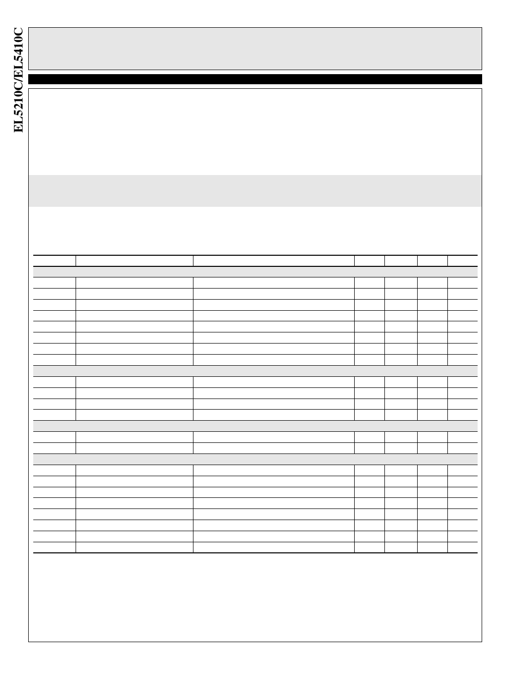
Electrical Characteristics
VS+ = +5V, VS - = -5V, RL = 1kΩ and CL = 12pF to 0V, TA = 25°C unless otherwise specified.
Parameter
Description
Input Characteristics
VOS
TCVOS
IB
RIN
CIN
CMIR
Input Offset Voltage
Average Offset Voltage Drift [1]
Input Bias Current
Input Impedance
Input Capacitance
Common-Mode Input Range
CMRR
Common-Mode Rejection Ratio
AVOL
Open-Loop Gain
Output Characteristics
VOL
Output Swing Low
VOH
Output Swing High
ISC
Short Circuit Current
IOUT
Output Current
Power Supply Performance
PSRR
Power Supply Rejection Ratio
IS
Supply Current (Per Amplifier)
Dynamic Performance
SR
Slew Rate [2]
tS
Settling to +0.1% (AV = +1)
BW
-3dB Bandwidth
GBWP
Gain-Bandwidth Product
PM
Phase Margin
CS
Channel Separation
dG
Differential Gain [3]
dP
Differential Phase[3]
VCM = 0V
VCM = 0V
Condition
for VIN from -5.5V to 5.5V
-4.5V ≤ VOUT ≤ 4.5V
IL = -5mA
IL = 5mA
VS is moved from ±2.25V to ±7.75V
No Load
-4.0V ≤ VOUT ≤ 4.0V, 20% o 80%
(AV = +1), VO = 2V Step
f = 5MHz
RF = RG = 1kΩ and VOUT = 1.4V
RF = RG = 1kΩ and VOUT = 1.4V
1. Measured over operating temperature range
2. Slew rate is measured on rising and falling edges
3. NTSC signal generator used
Min
Typ
Max Unit
3
15
mV
7
µ V/°C
2
60
nA
1
GΩ
2
pF
-5.5
+5.5
V
50
70
dB
65
80
dB
-4.9
-4.8
V
4.8
4.9
V
±120
mA
±30
mA
60
80
dB
2.5
3.75
mA
33
V/µ s
140
ns
30
MHz
20
MHz
50
°
110
dB
0.12
%
0.17
°
2
Share Link: 