IMS30 데이터 시트보기 (PDF) - Power-One Inc.
부품명
상세내역
제조사
IMS30 Datasheet PDF : 11 Pages
| |||
Input Transient Voltage Protection
A built-in suppressor diode provides effective protection
against input transients which may be caused for example
by short-circuits accross the input lines where the network
inductance may cause high energy pulses.
Table 3: Built-in transient voltage suppressor
Type
Breakdown
voltage
VBR nom [V]
Peak power
at 1 ms
PP [W]
Peak pulse
current
IPP [A]
48 IMS 30
100
600
4.1
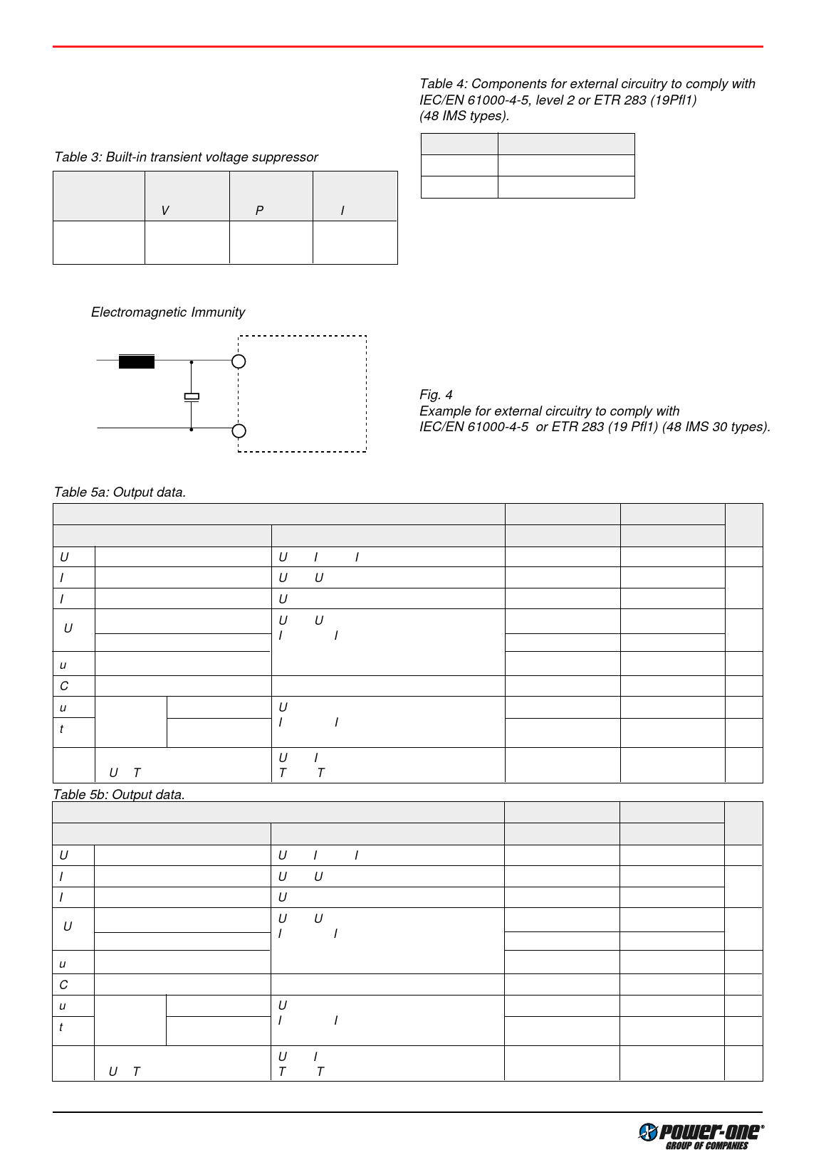
For very high energy transients as for example to achieve
IEC/EN 61000-4-5 or ETR 283 (19 Pfl1) compliance (as per
table: Electromagnetic Immunity) an external inductor and
capacitor are required.
04009
L
V+
1 Vi+
+
C
Module
V–
2 Vi–
Table 4: Components for external circuitry to comply with
IEC/EN 61000-4-5, level 2 or ETR 283 (19Pfl1)
(48 IMS types).
Circuit Ref.
L
C
48 IMS 30
150 uH
100 uF, 100 V, 85 C
Reverse Polarity Protection at the Input
The built-in suppressor diode also provides for reverse po-
larity protection at the input by conducting current in the re-
verse direction. An external fuse is required to limit this cur-
rent:
48 IMS 30: 3.15 A (F3.15A)
Fig. 4
Example for external circuitry to comply with
IEC/EN 61000-4-5 or ETR 283 (19 Pfl1) (48 IMS 30 types).
Electrical Ouput Data
Table 5a: Output data.
Model 48IMS30-0503-9G
Characteristics
Conditions
Uo1
Io nom
IoL
Uo
Output voltage
Output current
Current limit 1
Line regulation
Load regulation
Ui nom, Io = 0.5 Io nom
Ui min...Ui max
Ui nom
Ui min...Ui max
Io = (0...1) Io nom
uo1
Co ext
uo d
td
Output voltage noise 2
Admissible capacitive load
Dynamic
load
regulation
Voltage deviation
Recovery time
Ui nom
Io nom
1/2 Io nom
Uo Temperature coefficient
Uo/ TC
Table 5b: Output data.
Model 48IMS30-0302-9G
Ui nom, Io nom
TC min...TC max
Characteristics
Conditions
Uo1
Io nom
IoL
Uo
Output voltage
Output current
Current limit 1
Line regulation
Load regulation
Ui nom, Io = 0.5 Io nom
Ui min...Ui max
Ui nom
Ui min...Ui max
Io = (0...1) Io nom
uo1
Co ext
uo d
td
Output voltage noise 2
Admissible capacitive load
Dynamic
load
regulation
Voltage deviation
Recovery time
Ui nom
Io nom
1/2 Io nom
Uo Temperature coefficient
Ui nom, Io nom
Uo/ TC
TC min...TC max
1 The current limit is primary side controlled.
2 BW = 20 MHz
5.1 V
min typ max
5.00
5.20
0
3.5
6
+/-0.5
See Fig. 6
75
2000
250
1
3.3 V
min typ max Unit
3.25
3.35 V
0
6
A
9
+/-0.5 %
+/-1
50 mVpp
2000 uF
250 mV
1 ms
0.02
0.02 %/K
3.3 V
min typ max
3.25
3.35
0
4
6
+/-0.5
See Fig. 6
50
2000
250
1
1.8 V
min typ max
1.77
1.83
0
5
7
+/-0.5
+/-3
50
2000
150
1
Unit
V
A
%
mVpp
uF
mV
ms
0.02
0.02 %/K
4/11
Share Link: 