CDP68HC68A2 데이터 시트보기 (PDF) - Intersil
부품명
상세내역
제조사
CDP68HC68A2 Datasheet PDF : 14 Pages
| |||
CDP68HC68A2
Absolute Maximum Ratings
DC Supply Voltage Range, (VDD) . . . . . . . . . . . . . . . . . -0.5V to +7V
(Voltage Referenced to VSS Terminal)
Input Voltage Range, All Inputs . . . . . . . . . . . . . -0.5V to VDD +0.5V
DC Input Current, Any One Input . . . . . . . . . . . . . . . . . . . . . . . .±10mA
Operating Conditions (Note 1)
Temperature Ambient, TA . . . . . . . . . . . . . . . . . . . . . -40oC to 85oC
DC Voltage Range . . . . . . . . . . . . . . . . . . . . . . . . . . 3V Min, 6V Max
Thermal Information
Thermal Resistance (Typical, Note 2)
θJA (oC/W)
PDIP Package . . . . . . . . . . . . . . . . . . . . . . . . . . . . .
90
SOIC Package . . . . . . . . . . . . . . . . . . . . . . . . . . . . .
100
Maximum Power Dissipation Per Package
TA
TA
=
=
-40oC to 60oC (Package Type E)
60oC to 85oC (Package Type E)
.
Derate Linearly at. . . . . . . . . . . . . . . .
(PD)
............
. . . 12mW/oC
..
to
500mW
200mW
TA
TA
=
=
-40oC
-70oC
to
to
70oC
85oC
(Package
(Package
Derate Linearly at. . . . . . . .
Type
Type
....
M)
M)
...
(Note 3) . . . . . .
(Note 3)
. . . . 6.0mW/oC
..
to
400mW
310mW
Device Dissipation Per Output Transistor . . . . . . . . . . . . . . . . 40mW
TA = Full Package Temperate Range (All Package
Maximum Junction Temperature . . . . . . . . . . . . . . . . .
Types)
......
. 150oC
Maximum
Maximum
Storage Temperature Range (TSTG) . .
Lead Temperature (During Soldering).
.
.
.
.
.
.
-65oC
.....
to
..
150oC
265oC
At Distance 1/16 ±1/32 In. (1.59 ± 0.79mm)
From Case for 10s Max (SOIC - Lead Tips Only)
CAUTION: Stresses above those listed in “Absolute Maximum Ratings” may cause permanent damage to the device. This is a stress only rating and operation of the
device at these or any other conditions above those indicated in the operational sections of this specification is not implied.
NOTES:
1. For maximum reliability, nominal operating conditions should be selected so that operation is always within the ranges specified.
2. θJA is measured with the component mounted on a low effective thermal conductivity test board in free air. See Tech Brief TB379 for details.
3. Printed circuit board mount: 58mm x 57mm minimum area x 1.6mm thick G10 epoxy glass, or equivalent.
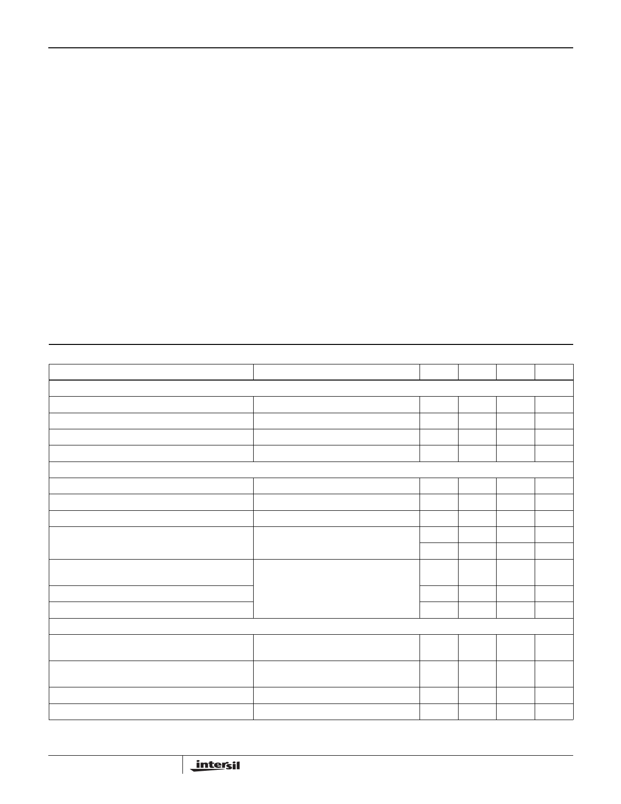
Electrical Specifications TA = 25oC, VDD = 5V, Unless Otherwise Specified.
PARAMETER
TEST CONDITIONS
ACCURACY
Differential Linearity Error
10-Bit Mode
Integral Linear Error
10-Bit Mode
Offset Error
10-Bit Mode
Gain Error
10-Bit Mode
ANALOG INPUTS: AI0 THRU AI7
Input Resistance
In Series with Sample Caps
Sample Capacitance
During Sample State
Input Capacitance
During Hold State
Input Current
At VIN = VREF + During Sample
During Hold or Standby State
Input + Full Scale Range
From Input RC Time Constant
VR = 1
Input Bandwidth (3dB)
Input Voltage Range: AI0
DIGITAL INPUTS: MOSI, SCK, CE, TA = -40oC to 85oC
High Input Voltage
VIH
VDD = 3 to 6V
Low Input Voltage
VIL
VDD = 3 to 6V
Input Leakage
Input Capacitance
TA = 25oC
MIN
TYP
MAX UNITS
-
±1.25
±2
LSB
-
±1.25
±2
LSB
-1
3
4
LSB
-1
1
2
LSB
-
85
-
Ω
-
400
-
pF
-
20
-
pF
-
+30
-
µA
-
-
±1
µA
VSS
-
VDD
V
+0.3
-
4.68
-
MHz
3.0
-
VDD
V
70
-
-
% of
VDD
-
-
30
% of
VDD
-
-
±1
µA
-
-
10
pF
3
Share Link: 