CDP68HC68A2 데이터 시트보기 (PDF) - Intersil
부품명
상세내역
제조사
CDP68HC68A2 Datasheet PDF : 14 Pages
| |||
CDP68HC68A2
$00
HIGH DATA REGISTER 0
$01
LOW DATA REGISTER 0
$0E
HIGH DATA REGISTER 7
$0F
LOW DATA REGISTER 7
DATA REGISTERS
$10
MODE SELECT REGISTER
$11
CHANNEL SELECT REGISTER
$12
START ADDRESS REGISTER
$13
STATUS REGISTER
A
OUT
IN
TO
D
AI0
8
AI1
TO
AI2
1
AI3
AI4
M
U
AI5
X
AI6
AI7
CHANNEL ADDRESS REGISTER
CONTROL/STATUS REGISTERS
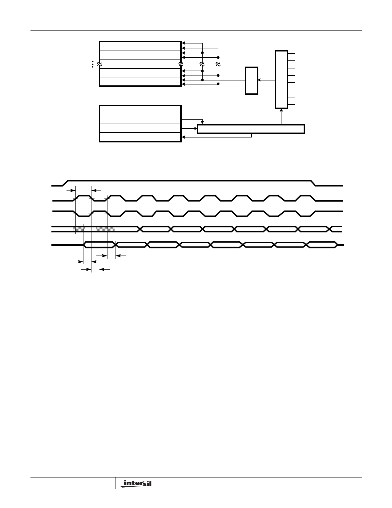
FIGURE 1. A PROGRAMMER’S MODEL OF THE CDP68HC68A2
CE
TP
SCKa
SCKb
MOSI
D7
D6
D5
D4
D3
D2
D1
D0
MISO
(READ
ONLY)
Tdsu
Tdh
Tdod
FIGURE 2. TIMING DIAGRAM FOR SERIAL PERIPHERAL INTERFACE
Serial Communications
Hardware Interface
All communications between the A2 and the controlling
processor are carried out over the Serial Peripheral Interface
(SPI) bus lines (MOSI, MISO, SCK, and CE). The SPI bus is
directly compatible with the SPI facilities of CDP68HC05
microcontrollers. Data is transmitted over the MISO and
MOSI lines synchronous with SCK. Transfers are done most
significant bit first.
The A2 acts as a “slave” device. The controlling “master”
signals the A2 that a SPI transfer is to take place by raising
CE and clocking SCK. A single shift register is used for
transferring data in and out of the A2. Whenever CE and
SCK are activated, data is shifted from the master to the A2
over the Master-Out-Slave-In (MOSI) line and,
simultaneously, during read operations, data is shifted to the
master from the A2 over the Master-In-Slave-Out (MISO)
line. Note that SCK must be provided by the master for both
reads and writes.
To accommodate various hardware systems, the A2 can
shift data on either the rising or falling edge of SCK. The
“active” edge is automatically determined by the A2. At the
moment that CE is first brought to a high level, the state of
SCK is latched. This latched state determines the
interpretation of SCK. If SCK is low when CE is activated,
data is shifted out on MISO on each rising edge of SCK and
data is latched from MOSI on each falling edge of SCK (see
SCKa in Figure 2). If SCK is high when CE is activated, data
is shifted out on MISO on each falling edge of SCK and data
is latched from MOSI on each rising edge of SCK (see SCKb
in Figure 2).
Hardware Interfacing to CDP68HC05 Controllers
When interfacing the A2 to CDP68HC05 controllers, set
CPHA = 1 and CPOL = (0 or 1) in the SPI control register. Note
that SCK pulses are generated only when data is written to the
SPI Data Register in a CDP68HC05. Reading data from or
writing data to the A2 requires writing data to the SPI Data
Register. The data will be ignored by the A2 for read operations.
The read data is available to the CDP68HC05 in the SPI Data
Register when SPIF is true in the SPI Status Register.
6
Share Link: 