CDP68HC68A2 데이터 시트보기 (PDF) - Intersil
부품명
상세내역
제조사
CDP68HC68A2 Datasheet PDF : 14 Pages
| |||
CDP68HC68A2
Hardware Interfacing to Non-CDP68HC05
Controllers
Most popular microcontrollers have a synchronous
communications facility which can be adapted to work with
the A2. Those that don’t can be easily interfaced using port
lines to synthesize a SPI bus.
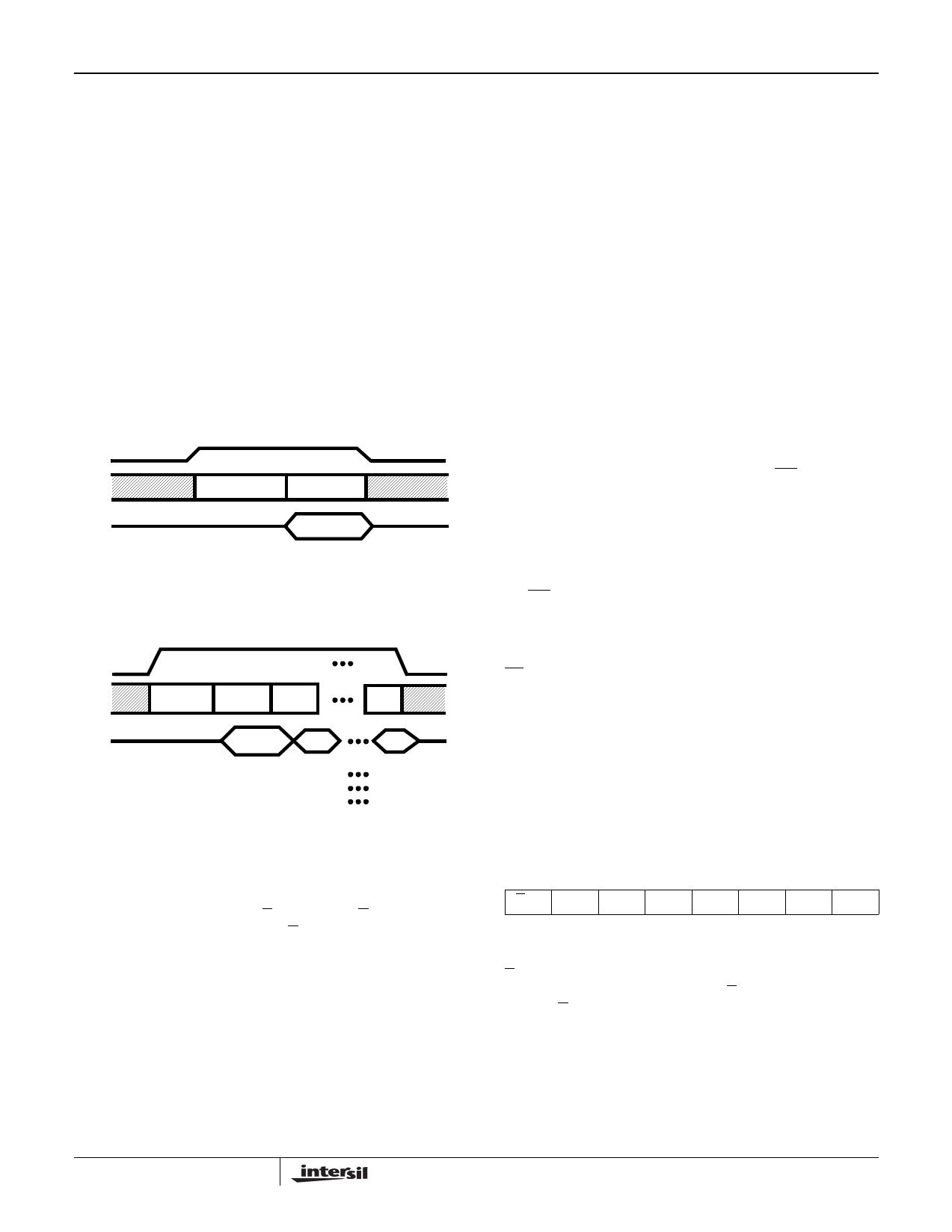
Software Interface
Reading and writing to the A2 can be performed in either
single byte or multiple byte (burst) modes. Both modes begin
the same way: a positive transition is applied to CE (if CE is
high, it must first be brought low, then returned high); an
address/control byte is transferred (requires 8 clocks on
SCK and 8 bits of data on MOSI); and the first byte of data is
transferred (requires 8 clocks of SCK). In the case of single
byte mode, the transfer is complete. For multiple byte
transfers, each series of 8 pulses on SCK produces another
8-bit transfer (see Figure 3).
CE
MOSI
ADDRESS BYTE DATA BYTE
MISO
HI - Z
READ
TRANSFER CYCLE:
PHASE:
1
2
I
II
FIGURE 3A. SINGLE BYTE TRANSFER
(REQUIRES 2 SPI TRANSFERS)
HI - Z
CE
MOSI
ADDRESS
BYTE
DATA
BYTE
DATA
DATA
MISO
HI - Z
READ
DATA
READ
HI - Z
READ
ADDRESS: WRITE ADDR: 1
TRANSFER CYCLE:
1
PHASE:
I
ADDR: 1 ADDR: 2
2
3
II
ADDR: N
N+1
II
FIGURE 3B. MULTIPLE (N) BYTE TRANSFER
(EFFICIENT DEVICE COMMUNICATION REQUIR-
ING N+1 SPI TRANSFERS)
The format of the address/control byte is shown in Figure 4.
The most significant bit is the R/W bit. When R/W is 0, read
operations are to be performed. If R/W is 1, write operations
are to be performed. A0 through A4 specify the register to
access. Data registers are mapped to address $00 through
$0F. The Control and Status Registers are at locations $10
through $13 (See Figure 1).
When transferring multiple bytes of data, the type of transfer
- read or write - is fixed by bit seven of the initial address/
control byte. After the initial data transfer, the address will
automatically be adjusted for each subsequent transfer.
When reading Data Registers in the 8-bit mode, each read
will advance the address by two, to the next (as specified in
the CSR) active channel’s Low Data Register. In the 10-bit
mode, following a read of a High Data Register, the address
is advanced to the Low Data Register of the same channel.
Reading the Low Data Register then increments the read
address to the next (as specified in the CSR) active chan-
nel’s High Data Register. Following a read of the last (closest
to 7) active channel’s Data Register(s), the address recycles
to the first (closest to 0) active channel’s Data Register(s).
When reading or writing control registers, the address will
increment to the next register after each transfer. Once
address $13 has been reached no more increments are
performed. This facilitates polling of the Status Register (SR)
which is located at address $13. If the A2 remains selected
following a read of SR, each successive 8 bit transfer will read
the SR again without; the need for an address /control byte.
Programming the CDP68HC68A2
Registers
Initializing the A2
The A2 is equipped with a power on reset circuit which
clears the MSR to all 0’s. This ensures that INT is in a high
impedance state and conversions are inhibited. The
contents of all other registers are unknown until explicitly
initialized. No other provisions are made for resetting the A2.
Systems which can be reset after power up must reset the
A2 by explicitly writing 0’s to the MSR. Designs which utilize
the INT line must be certain that the MSR is cleared, or the
A2 is initialized to a known state, before enabling interrupts.
NOTE: It is good practice to include code which initializes the A2, to
a known state, at the earliest practical point. In systems which utilize
INT, if a system reset occurs after power-up, A2 initialization code
must be executed before processor interrupts are enabled.
Address/Control Byte
The Address/Control Byte is a dual purpose word which
performs register addressing and read/write control. The
Address/Control Byte is the first byte transferred to the A2
following activation of CE. If CE is active, it must first be
brought low, then reactivated prior to transferring an
Address/Control Byte.
FIGURE 4. ADDRESS/CONTROL BYTE
R/W
-
-
A4 A3 A2 A1 A0
7
6
5
4
3
2
1
0
The most significant bit (MSB) of the Address/Control byte is
R/W. This bit is used to control the flow of data during the
subsequent SPI data transfers. If R/W is a 0, reads take
place. If R/W is a 1, writes take place. During read transfers,
data is shifted out on MISO. During writes, data is shifted in
on MOSI and MISO is held in a high impedance state.
The least significant five bits (A0 through A4) provide the
read address. Bits 5 and 6 are not required and can be sent
as either 0 or 1 (0’s are assembled throughout this
specification). When addressing Data Registers in 8-bit
7
Share Link: 