CMX838 데이터 시트보기 (PDF) - CML Microsystems Plc
부품명
상세내역
제조사
CMX838 Datasheet PDF : 71 Pages
| |||
FRS/PMR446/GMRS Family Radio Processor
CMX838
Package
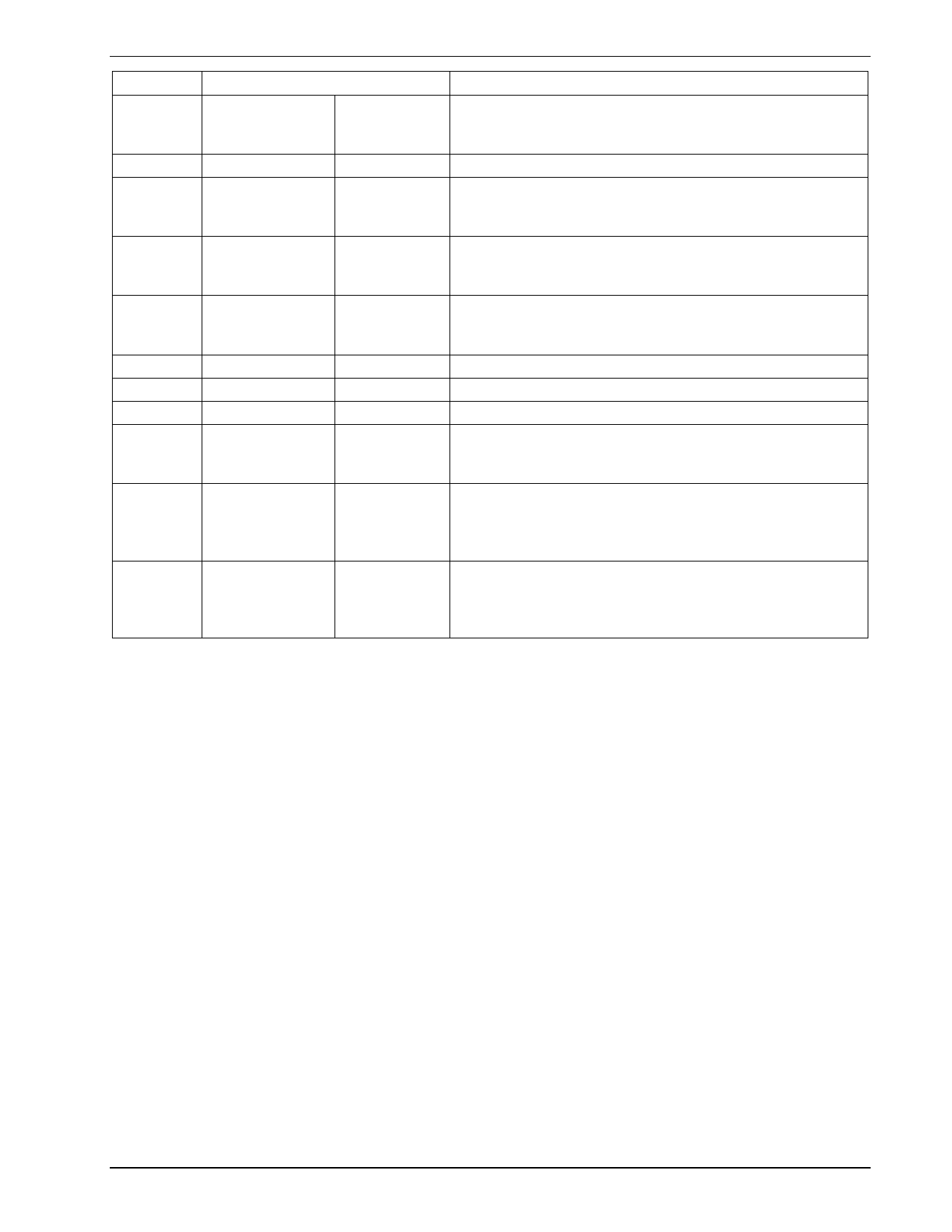
18
19
20
21
22
23
24
25
26
27
28
Signal
SERIAL CLOCK
input
VSS
TXMOD2
power
output
TXMOD1
output
VDD
RXOUT
BIN
AIN
VBIAS
BOUT
power
output
input
input
bi-directional
output
AOUT
output
Description
Serial clock input to C-BUS serial control port. This clock
input controls transfer timing of commands and data to
and from the device.
Negative supply (Circuit Common)
Transmit Output 2 internally switch selected to be at any
of (1) VBIAS, (2) transmit subaudio or (3) transmit audio
summed with subaudio.
Transmit Output 1 internally switch selected to be at any
of (1) VBIAS, (2) transmit audio or (3) transmit audio
summed with subaudio.
Positive supply. Levels and voltages are dependent upon
this supply. This signal must be decoupled to VSS by a
capacitor mounted close to the device pins.
Processed receive audio output.
External processing Path B input.
External processing Path A input.
A bias line for the internal circuitry, driven to VDD/2 by a
high impedance source. This signal must be decoupled by
a capacitor mounted close to the device pins.
External processing Path B output. This provides internal
switch controlled access to either Rx or Tx audio signals
for external processing such as expanding and
unscrambling.
External processing Path A output. This provides internal
switch controlled access to either Rx or Tx audio signals
for external processing such as compressing and
scrambling.
Table 1: Signal List
2003 CML Microsystems Plc
8
D/838/8
Share Link: 