CXA1851N 데이터 시트보기 (PDF) - Sony Semiconductor
부품명
상세내역
제조사
CXA1851N Datasheet PDF : 12 Pages
| |||
CXA1851N
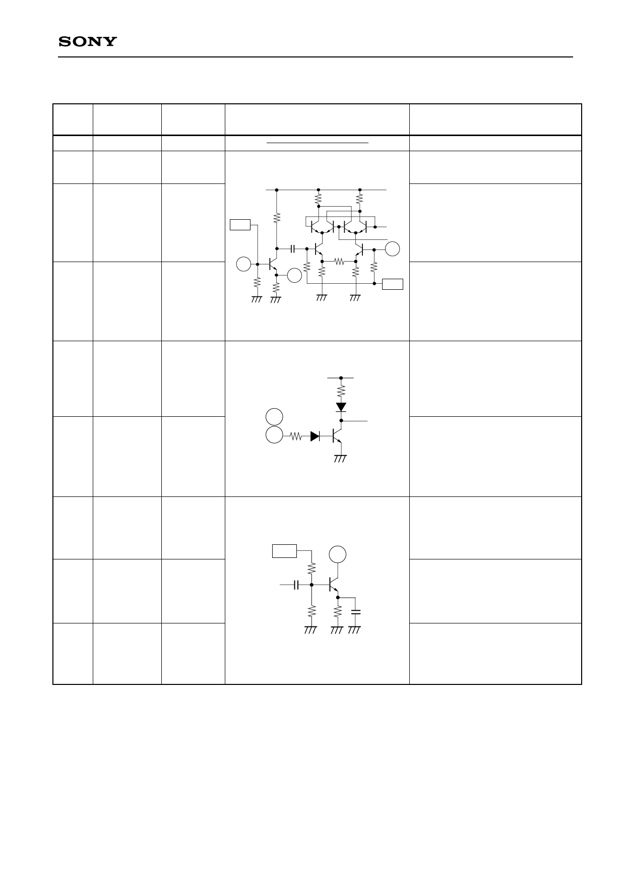
Pin Description
Pin No. Symbol
Typical pin
voltage (V)
1 GND
0.0
2 RF BYPASS 1.1
3 RF INPUT
0.9
Equivalent circuit
REG
4 PEAKING
0.12
3
4
OUT
5 P/S
(for DOWN
CONV.)
0 to 4.5
6 P/S
(for UP
CONV.)
0 to 4.5
7 VCC
(for Up
CONV.)
2.7 to 4.5
8 RF OUTPUT 2.7
(Vcc=2.7V)
9 GND
0.0
5
6
REG
8
Description
GND pin for the down converter.
MIX input by-pass pin for the down
converter.
RF input pin for the down
converter. Because of high
impedance, a 4.7 nH external chip
inductor should be used for
2 impedance matching.
Emitter pin for the low-noise
REG amplifier. Connect an approximate-
ly 3 pF chip capacitor and an
approximately 22Ω chip resistor in
series to the GND.
Power saving control pin for the
down converter.
OFF when Vp/s≤1.0 V; ON when
Vp/s≥1.8 V
Power saving control pin for the up
converter.
OFF when Vp/s≤1.0 V; ON when
Vp/s≥1.8 V
Power supply for the up converter.
RF output pin for the up converter.
Connect this pin to the Pin 7 power
supply via the 15 nH chip inductor.
GND pin for the up converter RF
amplifier.
—2—
Share Link: 