CXA2006 데이터 시트보기 (PDF) - Sony Semiconductor
부품명
상세내역
제조사
CXA2006 Datasheet PDF : 24 Pages
| |||
CXA2006Q
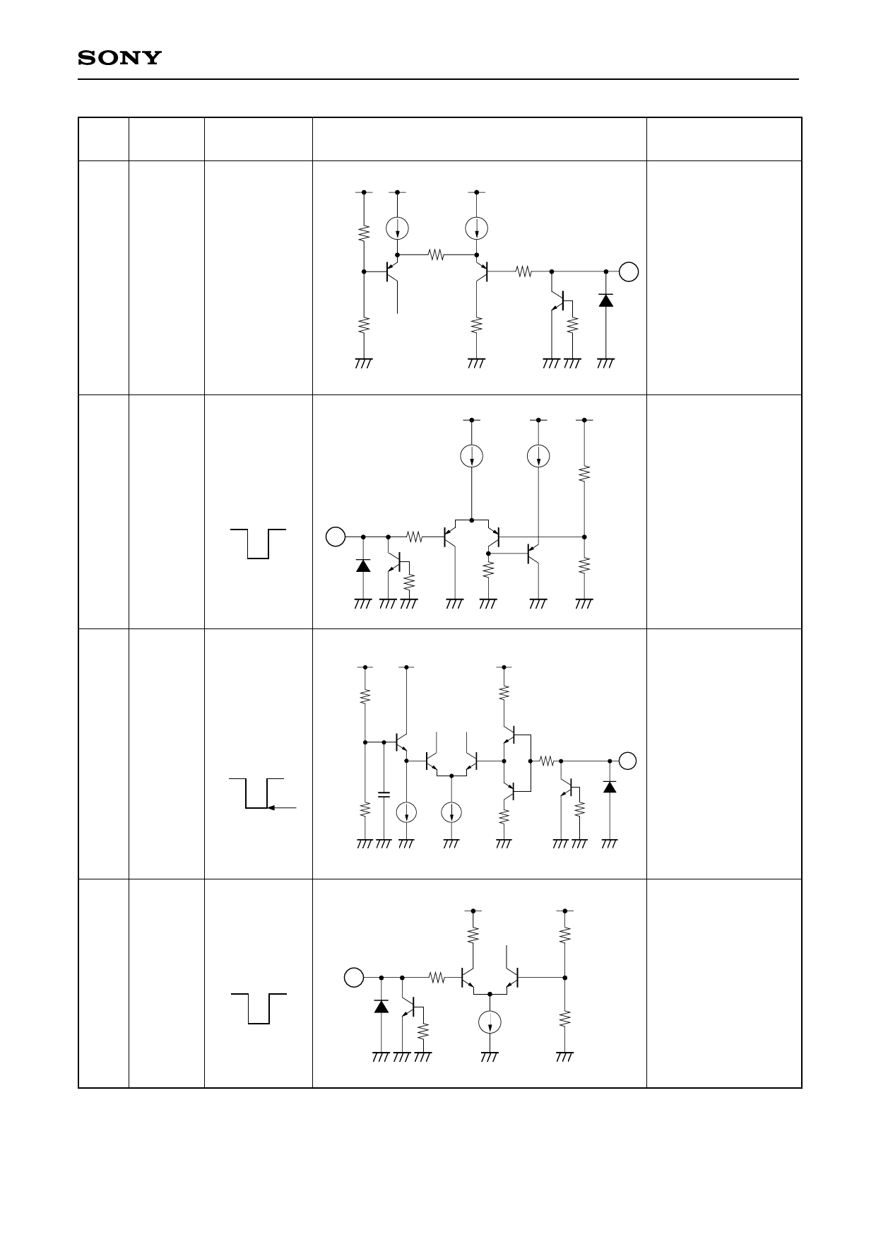
Pin
No.
Symbol
Pin voltage
66k
12 OFFSET
0 to 3V
24k
13 PBLK
VTH = 1.35V
13
Active: Low
Equivalent circuit
Description
100µA
23k
100µA
127
1.1k
Controls the output
offset during camera
mode.
12 When 0V:
less than
(VRB – 200mV)
10k
When 3.0V:
greater than
(VRB + 300mV)
127
10k
25µA
25µA
68k
1.35V
24k
27k
Camera signal pre-
blanking pulse input.
Active when Low only
during camera mode.
Calibrates the black
level of the AGC
output waveform.
When PBLK is Low,
the DRVOUT
potential is forced to
2V.
14 XRS
12.25k
VTH = 2.16V
2.16V
Sampling
10.25k
200
127
5p
100µA 2.5mA
200
Camera signal
sample-and-hold
14 pulse input.
10k
VTH = 1.45V
15 CLPOB
15
Active: Low
1.1k
127
10k
66k
1.45V
100µA
29k
Clamp pulse used to
clamp the optical
black portion of the
camera signal after it
passes through the
AGC amplifier.
–5–
Share Link: 