CXA2025 데이터 시트보기 (PDF) - Sony Semiconductor
부품명
상세내역
제조사
CXA2025 Datasheet PDF : 37 Pages
| |||
CXA2025AS
Pin
No.
Symbol
8 SDA
9 YUV SW
10 EYIN
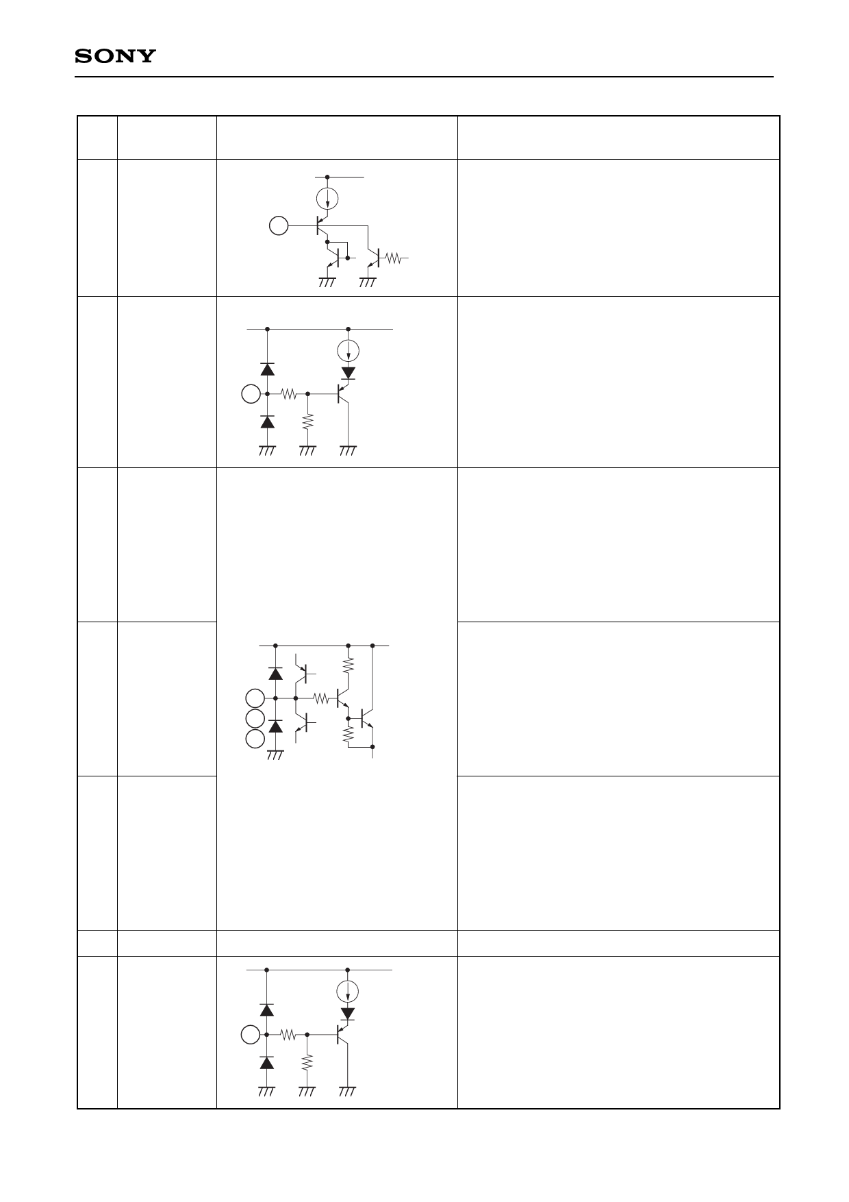
Equivalent circuit
JVCC
50µ
8
Description
I2C bus protocol SDA (Serial Data) I/O.
VILMAX = 1.5V
VIHMIN = 3.5V
VOLMAX = 0.4V
147
9
40k
SVCC
100µ
Switch control for the external YUV signal input.
When YUV SW is high, the external YUV signal
is selected; when YUV SW is low, the Y/C block
signal is selected. However, when the EY-SW
register is 1, the YIN (Pin 4) input is selected for
the Y signal even if YUV SW is high.
VILMAX = 0.4V
VIHMIN = 1.0V
VIHMAX = 3.0V
External Y signal input.
Input a 0.7Vp-p (100 IRE) Y signal via a
capacitor. The signal is clamped to 6.5V at the
burst timing of the signal input to the sync input
pin (Pin 44).
11 ERYIN
12 EBYIN
13 SGND
14 YM
SVCC
2k
1k
10
11
12
40k
147
14
40k
SVCC
100µ
External R-Y signal input.
Input a 0.78Vp-p (color difference signal
obtained by detecting a 100 IRE, 0.7Vp-p,
100% color bar chroma signal at the orthogonal
axis) + (R-Y) signal via a capacitor. The signal
is clamped to 6.2V at the burst timing of the
signal input to the sync input pin (Pin 44).
External B-Y signal input.
Input a 1.0Vp-p (color difference signal obtained
by detecting a 100 IRE, 0.7Vp-p, 100% color
bar chroma signal at the orthogonal axis) + (B-
Y) signal via a capacitor. The signal is clamped
to 6.2V at the burst timing of the signal input to
the sync input pin (Pin 44).
GND for the video block.
YM switch control input.
When YM is high, the Y/C block signal is
attennated by 6dB.
VILMAX = 0.4V
VIHMIN = 1.0V
VIHMAX = 3.0V
–4–
Share Link: 