CXA2025 데이터 시트보기 (PDF) - Sony Semiconductor
부품명
상세내역
제조사
CXA2025 Datasheet PDF : 37 Pages
| |||
CXA2025AS
Pin
No.
Symbol
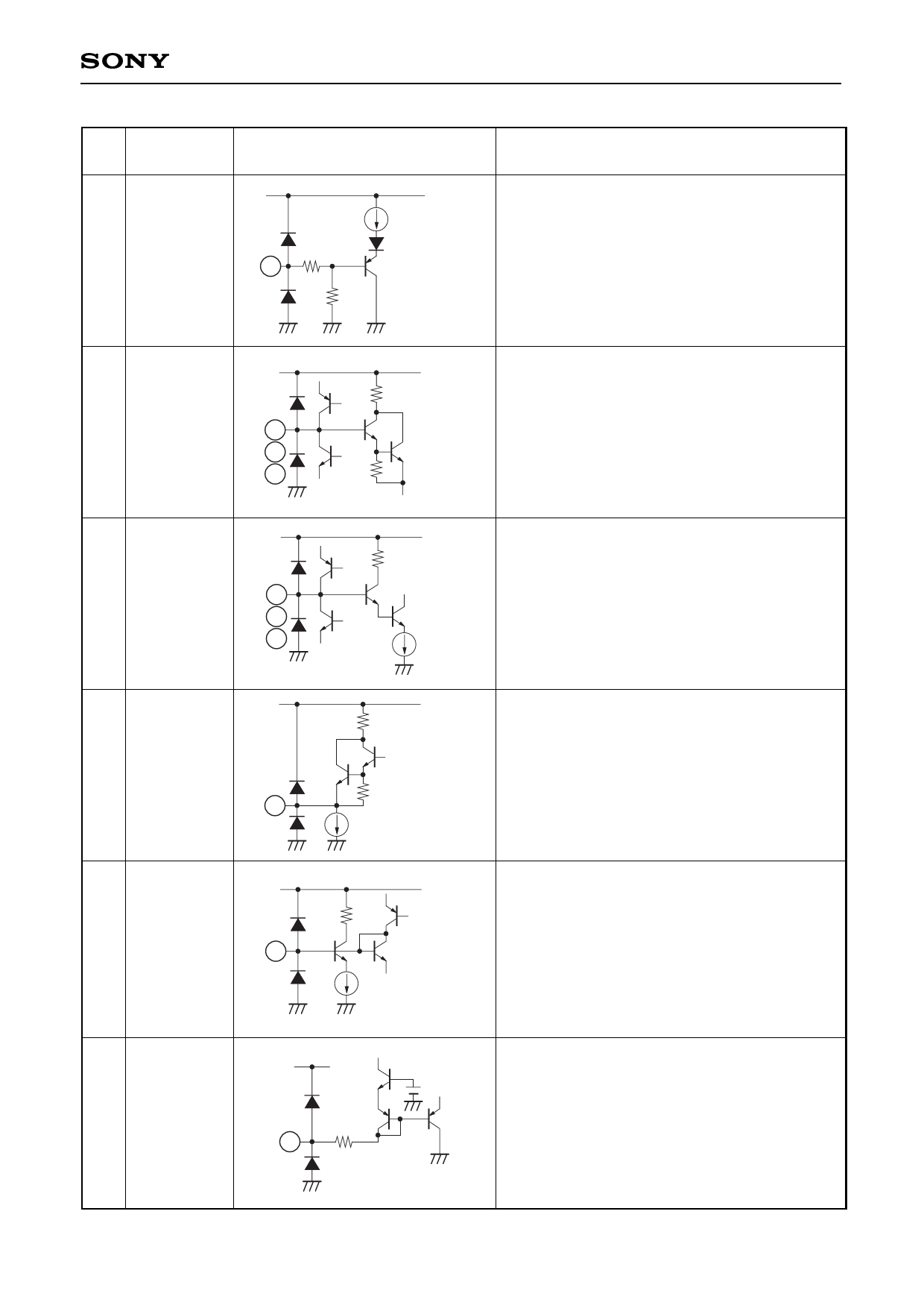
15 YS
16 RIN
17 GIN
18 BIN
19 RSH
21 GSH
23 BSH
20 ROUT
22 GOUT
24 BOUT
25 IKIN
26
ABLIN
/VCOMP
Equivalent circuit
147
15
40k
SVCC
100µ
Description
YS switch control input.
When YS is high, the RGB block signal is
selected; when YS is low, the Y/C block is
selected.
VILMAX = 0.4V
VIHMIN = 1.0V
VIHMAX = 3.0V
SVCC
200
Analog R, G and B signal input.
Input a 0.7Vp-p (no sync, 100 IRE) signal via a
16
capacitor. The signal is clamped to 5.1V at the
17
18
30k
burst timing of the signal input to the sync input
pin (Pin 44).
SVCC
1k
Sample-and-hold for R, G and B AKB.
Connect to GND via a capacitor. When not using
19
AKB (manual cut-off mode), R, G and B cut-off
21
voltage can be controlled by applying a control
23
voltage to each pin. The control voltage is 4.2 ±
50µ
2V.
SVCC
200
12k
20
1100µ
R, G and B signal output.
2.4Vp-p is output during 100% white input.
Input the signal converted from the CRT beam
SVCC
current (cathode current IK) to a voltage via a
1k
capacitor. The V blanking part is clamped to 2.7V at
the V retrace timing.
25
The input for this pin is the reference pulse return,
and the loop operates so that the Rch is 1Vp-p and
50µ
the G and Bch are 0.83Vp-p. The G and Bch can be
varied by ±0.5V by the bus CUTOFF control. When
not using AKB, this pin should not be connected.
SVCC
147
26
ABL control signal input and VSAW high voltage
fluctuation compensation signal input.
High voltage compensation has linear control
characteristics for the pin voltage range of about
3V to 1V.
ABL does not operate when the pin voltage is 9
[V], and operates with increasing strength as the
voltage becomes lower than 9 [V].
–5–
Share Link: 