CXA2025 데이터 시트보기 (PDF) - Sony Semiconductor
부품명
상세내역
제조사
CXA2025 Datasheet PDF : 37 Pages
| |||
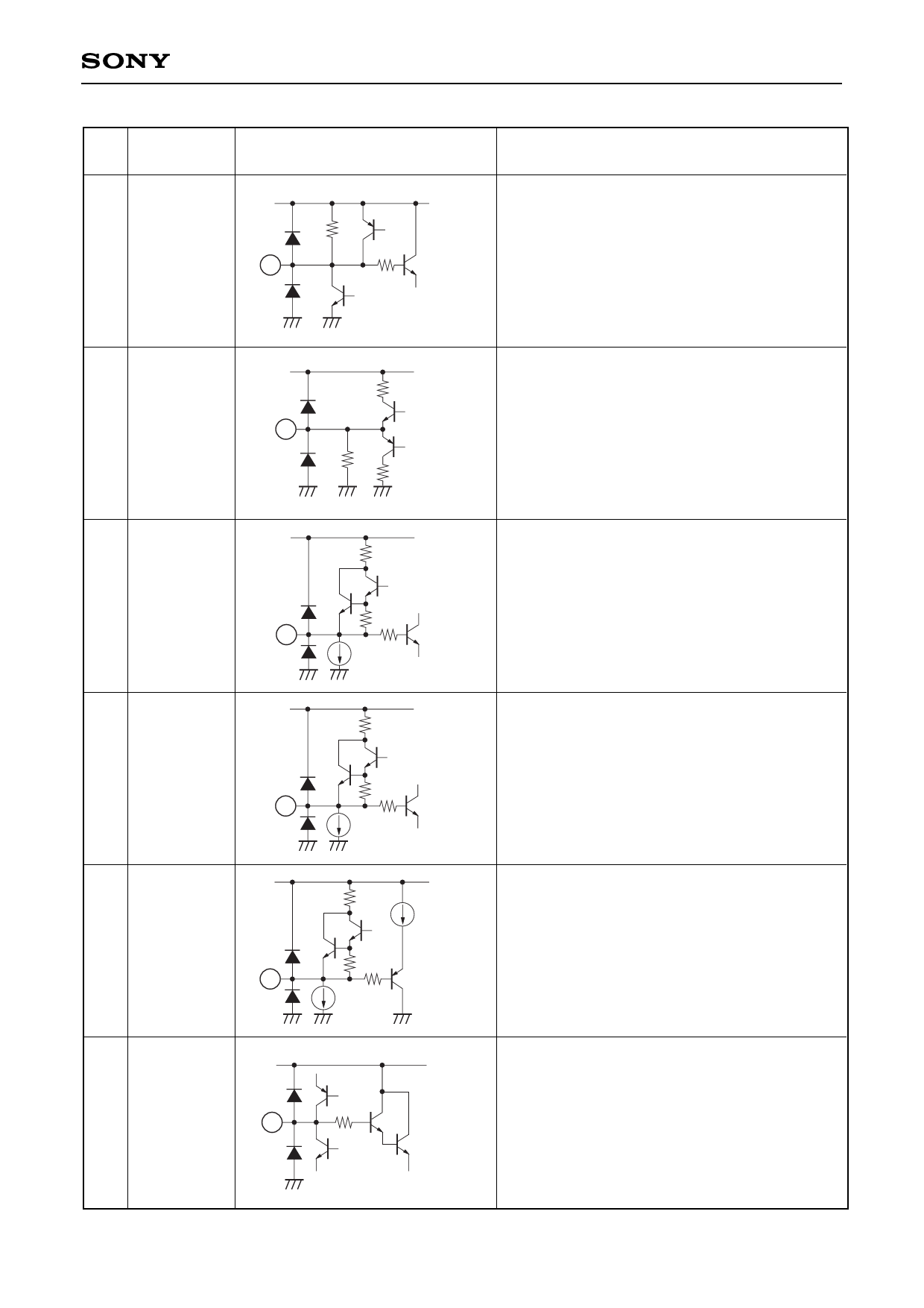
CXA2025AS
Pin
No.
Symbol
27 ABLFIL
Equivalent circuit
Description
10k
27
SVCC
1.2k
Connect a capacitor to form the LPF of the ABL
control signal.
28
VTIM
(SCP)
29
VDRIVE–
/VPROT
30
VDRIVE+
/VPROT
31 EWDRIVE
1k
28
10k
1k
JVCC
JVCC
720
30k
29
24k
400µ
V timing pulse output.
Outputs the timing pulse from V sync
identification to the end of V blanking. Pulses are
positive polarity from 0 to 6 [V]. During zoom
mode, the V blanking pulse which has been
expanded before and after the V sync is
superimposed and output as the 0 to 3 [V] pulse.
V sawtooth wave output and Vprotect signal
input.
When a large current (3mA) is led from this pin,
the RGB outputs are all blanked and the status
is returned to the I2C bus.
JVCC
720
30k
30
24k
400µ
Outputs a V sawtooth wave of the opposite
polarity as VDRIVE–. The Vprotect function can
also be operated by this pin.
JVCC
1.4k
25µ
15k
31
78k
800µ
V parabola wave output.
32 VAGCSH
1.2k
32
JVCC
Sample-and-hold for AGC which maintains the V
sawtooth wave at a constant amplitude.
Connect to GND via a capacitor.
–6–
Share Link: 