CXA2093 데이터 시트보기 (PDF) - Sony Semiconductor
부품명
상세내역
제조사
CXA2093 Datasheet PDF : 11 Pages
| |||
CXA2093S
Electrical Characteristics
(Ta = 25°C, VCC = 5V)
No.
Item
Symbol
Measure-
ment pins
Input signals
Measurement contents
Min. Typ. Max. Unit
1
Power
consumption
ICC
6
16
18
Vcc pin inflow current
45 69 95 mA
2 I/O gain R
3 I/O gain G
4 I/O gain B
VGR 21
Input video signal to Pins 1, 3 and
5, input clamp pulse to Pin 13, and
–0.5
0.5
VGG
19
Pins 1, 3, 5: Sig-1
Pin 13: Sig-2
measure the output amplitude of
each output pin. Then calculate
the I/O gain.
–0.5
0.5
VGB 17
VGR = 20 log
output amplitude
0.7
–0.5
0.5
1.5 dB
1.5 dB
1.5 dB
5
Input dynamic
range
Drng
17
19
21
Pins 1, 3, 5: Sig-3
Pin 13: Sig-2
Input video signal to Pins 1, 3 and 5, input
clamp pulse to Pin 13, and measure the
output amplitude of each output pin.
0.9
1.05
1.2 Vp-p
6
Sharpness
gain 1
Pins 1, 3, 5: CW Input 30MHz and 0.1Vp-p sine wave
VSG1 19 Pin 13: 5 V
to Pins 1, 3 and 5, and measure the 60
Pin 12: 0.5 V output amplitude of Pin 19.
110 150 mVp-p
7
Sharpness
gain 2
Input 30MHz and 0.1Vp-p sine wave
to Pins 1, 3 and 5, and measure the
Pins 1, 3, 5: CW output amplitude of Pin 19. Then
VSG2 19 Pin 13: 5 V
calculate the I/O gain.
5.0 7.0 9.0 dB
Pin 12: 2.5 V
VGR = 20 log
output amplitude
0.1
8
Sharpness
gain 3
Pins 1, 3, 5: CW Input 30MHz and 0.1Vp-p sine wave
VSG3 19 Pin 13: 5 V
to Pins 1, 3 and 5, and measure the 60
Pin 12: 3.0 V output amplitude of Pin 19.
110 150 mVp-p
9
Sharpness
gain 4
Input 30MHz and 0.1Vp-p sine wave
VSG4 19
Pins 1, 3, 5: CW
Pin 13: 5 V
Pin 12: 4.5 V
to Pins 1, 3 and 5, and measure the
output amplitude of Pin 19. Then
calculate the I/O gain.
5.0
7.0
9.0 dB
VGR = 20 log
output amplitude
0.1
10
DIFOUT
output level
Pin 1: CW
VDF 15 Pin 13: 5 V
Pin 12: 4.5 V
Input 30MHz and 0.3Vp-p sine
wave to Pin 1, and measure the 290 375 455 mVp-p
output amplitude of Pin 15.
11
SYNCSEP
output high level
VSHi
Input video signal to Pin 7, and
measure the high level of Pin 14.
3.9
4.2
4.5
V
12
SYNCSEP
output low level
VSLo
14
Pin 7: Sig-4
13
SYNCSEP
output delay 1
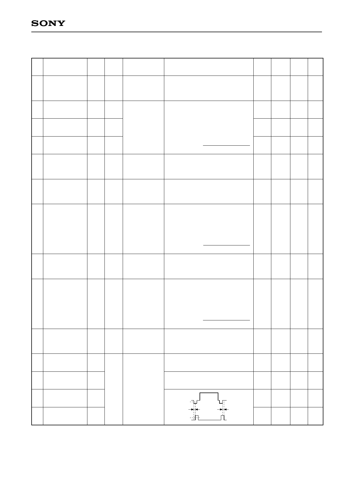
SDtr
14
SYNCSEP
output delay 1
SDtf
Input video signal to Pin 7, and
measure the low level of Pin 14.
0.1
0.18 0.26
V
Vth = 50%
SDtr
SDtf
Vth = 50%
0 19 40 ns
30 51 70 ns
–5–
Share Link: 