CXD2453Q 데이터 시트보기 (PDF) - Sony Semiconductor
부품명
상세내역
제조사
CXD2453Q Datasheet PDF : 21 Pages
| |||
CXD2453Q
The following provides a detailed description of each setting.
(a) Setting of PLL counter frequency division ratio
This is used to set the frequency division ratio of the 1/N frequency divider (PLL counter) for phase
comparison. The value of (total number of dots of 1 horizontal period N) – 1 is set with PLP10 (MSB) through
PLP0 (LSB). The frequency division ratio can be set up to 2048. Only even numbers can be set for the value of
N. When it is necessary to set an odd number, use an external frequency divider. In this case, set the value of
the frequency division ratio of the PLL counter to N-2.
The default value is 10100111111 (N = 1344).
(b) Setting of screen horizontal position
The horizontal display start position is set with HP7 (MSB) through HP0 (LSB). This setting enables the phase
relationships of pulses HST, HCK1/2, ENB, PCG, PRG and CLP1/2 as well as the changing positions of
VCK/FRP relative to HSYNC to change in an interlocked manner. Settings can be made in 1 dot units. Refer to
the Timing Chart for the relationship between the set value and each pulse position.
The default value is 01000100.
(c) Setting of screen vertical position
The vertical display start position is set with VP7 (MSB) through VP0 (LSB). This setting enables the phase
relationships of signals VST, VCK and FRP to change relative to VSYNC in an interlocked manner. Settings
can be made in 1 line units. Refer to the Timing Chart for the relationship between the set value and each
signal.
The default value is 00100011. 00000000 and 11111111 are not used.
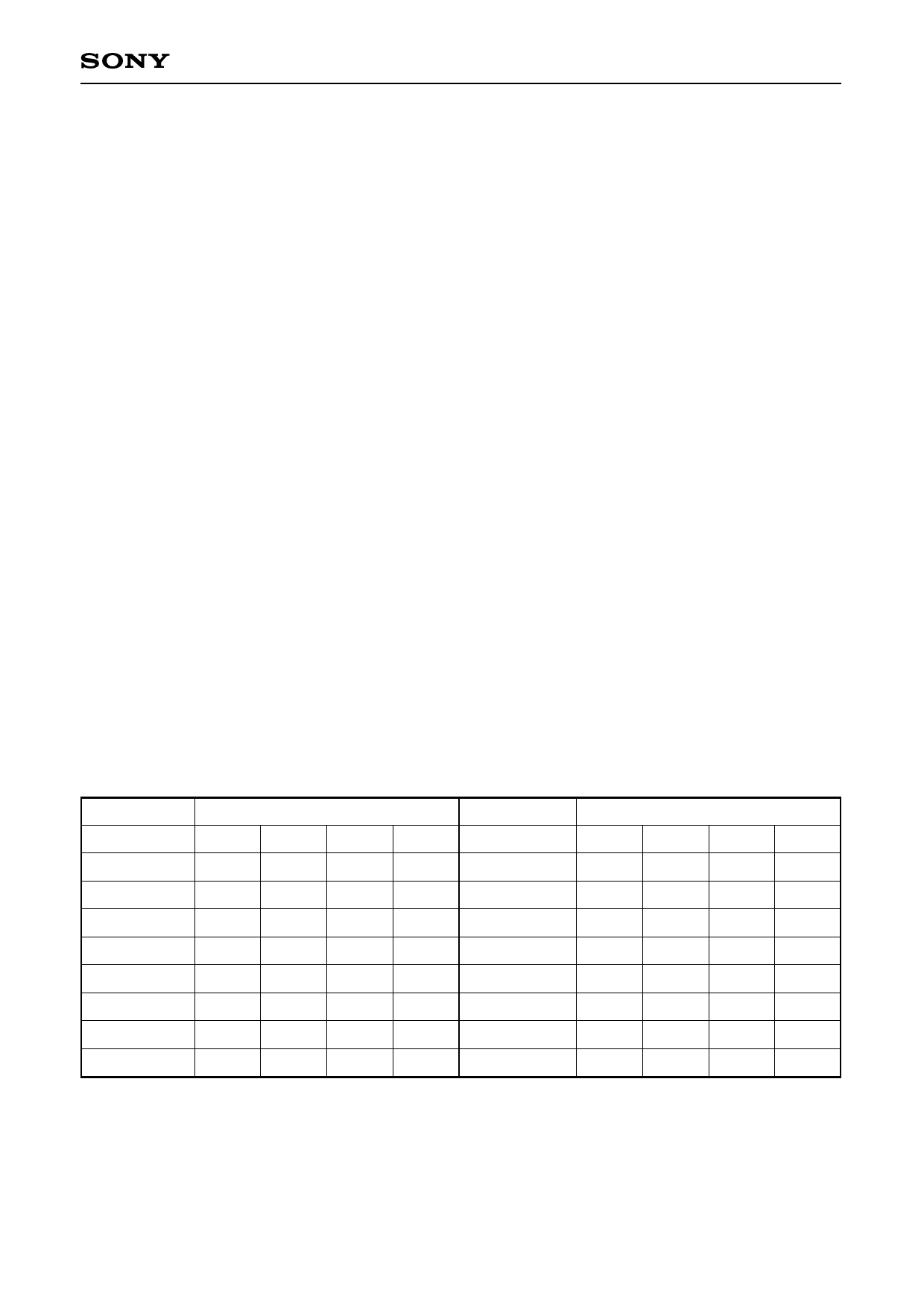
(d) S/H control of CXA2112R
This is used to set the sample-and-hold position for the CXA2112R (sample-and-hold driver). INV setting data
is output directly from the INV (Pin 60). Setting data of SHP3 (MSB) through SHP0 (LSB) is reflected as shown
below in the SHPA through SHPD (Pins 56 to 59). Refer to the specifications of the CXA2112R for details.
Setting data
Output
SHP3 to SHP0 SHPA SHPB SHPC
0000
0001
0010
0011
0100
0101
0110
0111
L
L
L
H
H
L
Z
L
L
Z
H
L
L
L
H
H
H
H
Z
L
H
Z
H
H
Note) Z: High impedance state
Setting data
SHPD SHP3 to SHP0 SHPA
L
1000
L
L
1001
H
L
1010
Z
L
1011
Z
H
1100
L
H
1101
H
H
1110
Z
H
1111
Z
Output
SHPB SHPC
L
Z
H
Z
L
Z
H
Z
L
Z
H
Z
L
Z
H
Z
SHPD
L
L
L
L
H
H
H
H
– 11 –
Share Link: 