CY62256VN(2011) 데이터 시트보기 (PDF) - Cypress Semiconductor
부품명
상세내역
제조사
CY62256VN Datasheet PDF : 14 Pages
| |||
CY62256VN
256K (32K × 8) Static RAM
256K (32K × 8) Static RAM
Features
■ Temperature ranges
❐ Commercial: 0 °C to +70 °C
❐ Industrial: –40 °C to +85 °C
❐ Automotive-A: –40 °C to +85 °C
❐ Automotive-E: –40 °C to +125 °C
■ Speed: 70 ns
■ Low voltage range: 2.7 V to 3.6 V
■ Low active power and standby power
■ Easy memory expansion with CE and OE features
■ TTL compatible inputs and outputs
■ Automatic power down when deselected
■ CMOS for optimum speed and power
■ Available in standard Pb-free and non Pb-free 28-pin (300-mil)
narrow SOIC, 28-pin TSOP-I, and 28-pin reverse TSOP-I
packages
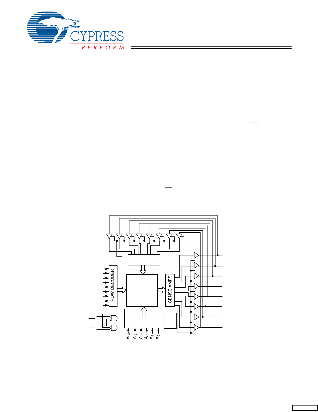
Logic Block Diagram
Functional Description
The CY62256VN[1] family is composed of two high performance
CMOS static RAM’s organized as 32K words by 8 bits. Easy
memory expansion is provided by an active LOW chip enable
(CE) and active LOW output enable (OE) and tristate drivers.
These devices have an automatic power down feature, reducing
the power consumption by over 99% when deselected.
An active LOW write enable signal (WE) controls the
writing/reading operation of the memory. When CE and WE
inputs are both LOW, data on the eight data input/output pins
(I/O0 through I/O7) is written into the memory location addressed
by the address present on the address pins (A0 through A14).
Reading the device is accomplished by selecting the device and
enabling the outputs, CE and OE active LOW, while WE remains
inactive or HIGH. Under these conditions, the contents of the
location addressed by the information on address pins are
present on the eight data input/output pins.
The input/output pins remain in a high impedance state unless
the chip is selected, outputs are enabled, and write enable (WE)
is HIGH.
I/O0
INPUTBUFFER
A10
I/O1
A9
A8
I/O2
A7
A6
A5
32K x 8
ARRAY
I/O3
A4
I/O4
A3
A2
I/O5
CE
WE
COLUMN
DECODER
POWER
DOWN
I/O6
OE
I/O7
.
Note
1. For best practice recommendations, refer to the Cypress application note “System Design Guidelines” on http://www.cypress.com.
Cypress Semiconductor Corporation • 198 Champion Court
Document Number: 001-06512 Rev. *D
• San Jose, CA 95134-1709 • 408-943-2600
Revised January 4, 2011
[+] Feedback
Share Link: 