CY7C1021CV33-10ZSXA 데이터 시트보기 (PDF) - Cypress Semiconductor
부품명
상세내역
제조사
CY7C1021CV33-10ZSXA Datasheet PDF : 14 Pages
| |||
CY7C1021CV33
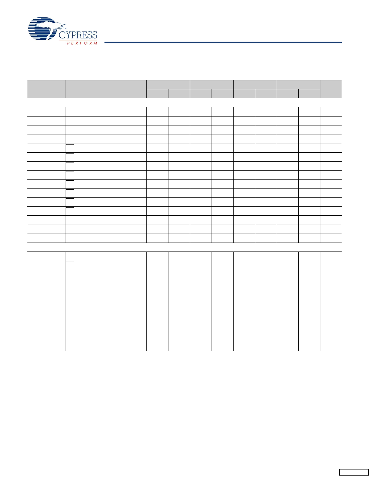
Switching Characteristics
Over the Operating Range [5]
Parameter
Description
Read Cycle
tpower[6]
VCC(Typical) to the First Access
tRC
Read Cycle Time
tAA
Address to Data Valid
tOHA
Data Hold from Address Change
tACE
CE LOW to Data Valid
tDOE
tLZOE
tHZOE
tLZCE
tHZCE
tPU[9]
tPD[9]
OE LOW to Data Valid
OE LOW to Low Z[7]
OE HIGH to High Z[7, 8]
CE LOW to Low Z[7]
CE HIGH to High Z[7, 8]
CE LOW to Power Up
CE HIGH to Power Down
tDBE
Byte Enable to Data Valid
tLZBE
Byte Enable to Low Z
tHZBE
Byte Disable to High Z
Write Cycle[10]
tWC
tSCE
tAW
tHA
tSA
tPWE
tSD
tHD
tLZWE
tHZWE
tBW
Write Cycle Time
CE LOW to Write End
Address Setup to Write End
Address Hold from Write End
Address Setup to Write Start
WE Pulse Width
Data Setup to Write End
Data Hold from Write End
WE HIGH to Low Z[7]
WE LOW to High Z[7, 8]
Byte Enable to End of Write
-8
Min Max
100
8
8
3
8
5
0
4
3
4
0
8
5
0
4
8
7
7
0
0
6
5
0
3
4
6
-10
Min Max
100
10
10
3
10
5
0
5
3
5
0
10
5
0
5
10
8
8
0
0
7
5
0
3
5
7
-12
Min Max
100
12
12
3
12
6
0
6
3
6
0
12
6
0
6
12
9
9
0
0
8
6
0
3
6
8
-15
Min Max
100
15
15
3
15
7
0
7
3
7
0
15
7
0
7
15
10
10
0
0
10
8
0
3
7
9
Unit
μs
ns
ns
ns
ns
ns
ns
ns
ns
ns
ns
ns
ns
ns
ns
ns
ns
ns
ns
ns
ns
ns
ns
ns
ns
ns
Notes
5. Test conditions assume signal transition time of 3 ns or less, timing reference levels of 1.5V, and input pulse levels of 0 to 3.0V.
6. tPOWER gives the minimum amount of time that the power supply is at typical VCC values until the first memory access is performed.
7. At any temperature and voltage condition, tHZCE is less than tLZCE, tHZOE is less than tLZOE, and tHZWE is less than tLZWE for any given device.
8. tHZOE, tHZBE, tHZCE, and tHZWE are specified with a load capacitance of 5 pF as in part (d) of “AC Test Loads and Waveforms” on page 5. Transition is measured ±500
mV from steady state voltage.
9. This parameter is guaranteed by design and is not tested.
10. The internal write time of the memory is defined by the overlap of CE LOW, WE LOW, and BHE/BLE LOW. CE, WE, and BHE/BLE is LOW to initiate a write. The
transition of these signals terminate the write. The input data setup and hold timing is referenced to the leading edge of the signal that terminates the write.
Document Number: 38-05132 Rev. *I
Page 6 of 14
[+] Feedback
Share Link: 