CY7C1340A-66 데이터 시트보기 (PDF) - Cypress Semiconductor
부품명
상세내역
제조사
CY7C1340A-66 Datasheet PDF : 12 Pages
| |||
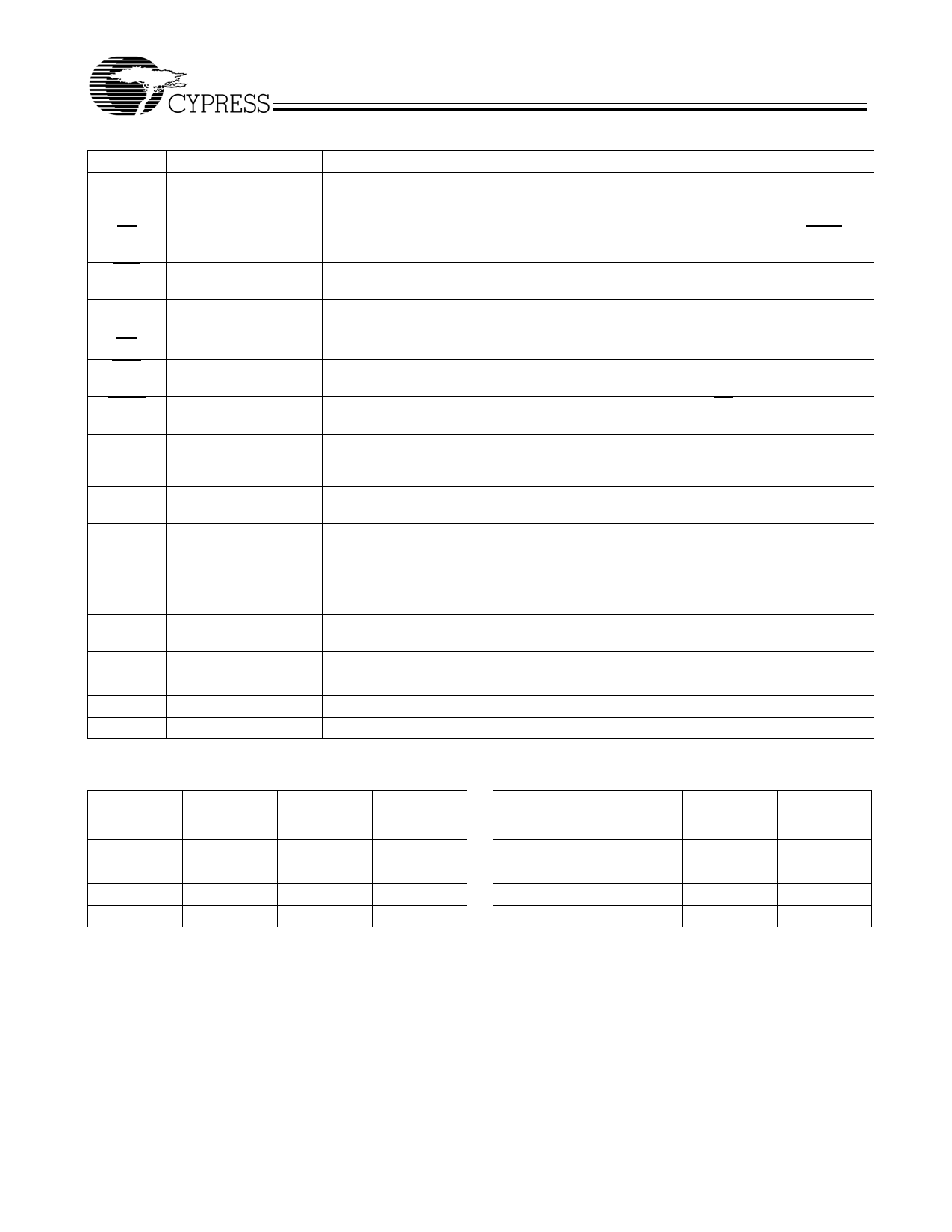
Pin Descriptions
Name
CLK
Type
Input-
Synchronous
CE
CE2
CE2
OE
ADV
ADSP
ADSC
Input-
Synchronous
Input-
Synchronous
Input-
Synchronous
Input
Input-
Synchronous
Input-
Synchronous
Input-
Synchronous
MODE
ZZ
DQ1–
DQ32
Input-
Static
Input-
Asynchronous
Input/
Output
VCC
VSS
VCCQ
VSSQ
NC
Supply
Ground
I/O Supply
I/O Ground
-
CY7C1340A
Description
Clock: This signal registers the addresses, data, chip enables, Write control and burst
control inputs on its rising edge. All synchronous inputs must meet set-up and hold times
around the clock’s rising edge.
Chip Enable: This active LOW input is used to enable the device and to gate ADSP.
Chip Enable: This active LOW input is used to enable the device.
Chip Enable: This active HIGH input is used to enable the device.
Output Enable: This active LOW asynchronous input enables the data output drivers.
Address Advance: This active LOW input is used to control the internal burst counter.
A HIGH on this pin generates wait cycle (no address advance).
Address Status Processor: This active LOW input, along with CE being LOW, causes a
new external address to be registered and a Read cycle is initiated using the new address.
Address Status Controller: This active LOW input causes device to be de-selected or
selected along with new external address to be registered. A Read or Write cycle is initiated
depending upon Write control inputs.
Mode: This input selects the burst sequence. A LOW on this pin selects Linear Burst. A NC
or HIGH on this pin selects Interleaved Burst.
Snooze: This active HIGH input puts the device in low power consumption standby mode.
For normal operation, this input has to be either LOW or NC (No Connect).
Data Inputs/Outputs: First Byte is DQ1–DQ8. Second Byte is DQ9–DQ16. Third Byte is
DQ17–DQ24. Fourth Byte is DQ25–DQ32. Input data must meet set-up and hold times
around the rising edge of CLK.
Power Supply: +3.3V –5% to +10%. Pin 14 does not have to be connected directly to
VCC as long as it is greater than VIH.
Ground: GND
Output Buffer Supply: +3.3V –5% to +10%. For 2.5V I/O: 2.375V to VCC.
Output Buffer Ground: GND
No Connect: These signals are not internally connected.
Burst Address Table (MODE = NC/VCC)
First
Address
(external)
Second
Address
(internal)
Third
Address
(internal)
Fourth
Address
(internal)
A...A00
A...A01
A...A10
A...A11
A...A01
A...A00
A...A11
A...A10
A...A10
A...A11
A...A00
A...A01
A...A11
A...A10
A...A01
A...A00
Burst Address Table (MODE = GND)
First
Address
(external)
A...A00
A...A01
A...A10
A...A11
Second
Address
(internal)
A...A01
A...A10
A...A11
A...A00
Third
Address
(internal)
A...A10
A...A11
A...A00
A...A01
Fourth
Address
(internal)
A...A11
A...A00
A...A01
A...A10
Document #: 38-05153 Rev. *C
Page 4 of 12
Share Link: 