SA5522 데이터 시트보기 (PDF) - Philips Electronics
부품명
상세내역
제조사
SA5522 Datasheet PDF : 20 Pages
| |||
Philips Semiconductors
1.4 GHz I2C-bus controlled synthesizer
Product specification
TSA5522
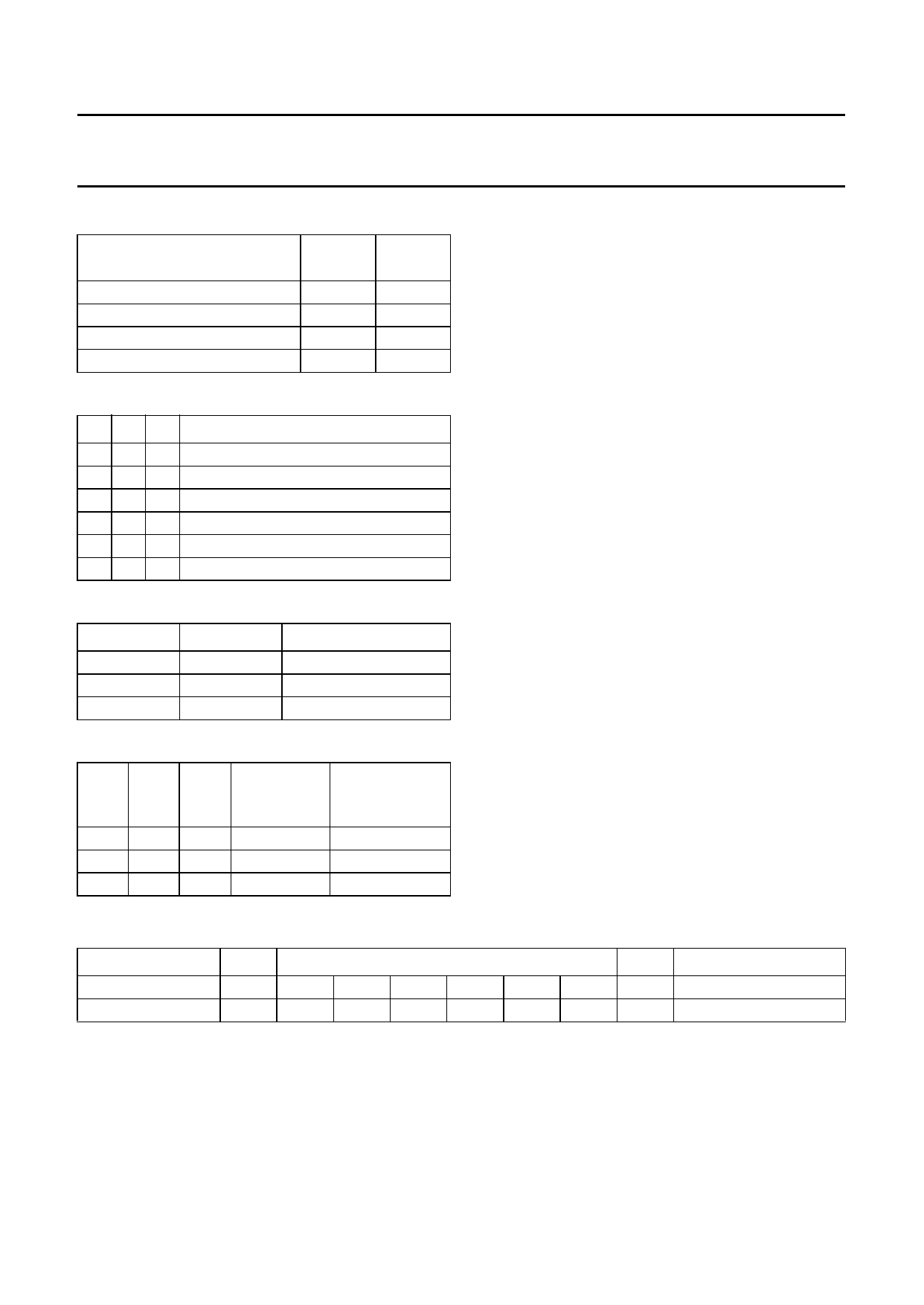
Table 3 Address selection
VOLTAGE APPLIED ON AS
INPUT
0 to 0.1VCC1
Always valid
0.4VCC1 to 0.6VCC1
0.9VCC1 to VCC1
MA1
0
0
1
1
MA2
0
1
0
1
Table 4 Test bits
T2 T1 T0
DEVICE OPERATION
0 0 1 normal mode
0 1 X charge-pump is OFF
1 1 0 charge-pump is sinking current
1 1 1 charge-pump is sourcing current
1 0 0 fref is available at LOCK output
1 0 1 1⁄2fdiv is available at LOCK output
Table 5 Ratio select bits
RSA
X
0
1
RSB
0
1
1
REFERENCE DIVIDER
640
1 024
512
Table 6 Band switch output levels
VOLTAGE
P2 P1 P0
ON BS
OUTPUT
0
1
0
0.25 V
1
0
0
0.4VCC1
0
0
1
0.8VCC1
PHILIPS M/O
BAND
band A
band B
band C
READ MODE; R/W = 1 (see Table 7)
Data can be read from the device by setting the R/W bit to
logic 1. After the slave address has been recognized, the
device generates an acknowledge pulse and the first data
byte (status byte) is transferred on the SDA line (MSB
first). Data is valid on the SDA line during a HIGH level of
the SCL clock signal. A second data byte can be read from
the device if the microcontroller generates an
acknowledge on the SDA line (master acknowledge). End
of transmission will occur if no master acknowledge
occurs. The device will then release the data line to allow
the microcontroller to generate a STOP condition. When
ports P4 to P7 are used as inputs, the corresponding bits
must be logic 0 (high impedance state). The POR flag is
set to logic 1 at power-on. The flag is reset when an
end-of-data is detected by the device (end of a read
sequence). Control of the loop is made possible with the
in-lock flag (FL) which indicates when the loop is locked
(FL = 1).
The bits I2, to I0 represent the status of the I/O ports
P7, P5 and P4 respectively. A logic 0 indicates a LOW
level and a logic 1 indicates a HIGH level
(see “Characteristics”).
A built-in ADC is available at pin P6. This converter can be
used to apply AFC information to the microcontroller from
the IF section of the television. The relationship between
the bits A2 to A0 is given in Table 8.
Table 7 READ data format
BYTE
MSB
DATA BYTE
Address byte (ADB) 1
1
0
0
0
MA1
Status byte (SB)
POR(2) FL(3) I2(4)
I1(4)
I0(4) A2(5)
Notes
1. A = acknowledge.
2. POR = power-on-reset (POR = 1 at power-on).
3. FL = in-lock flag (FL = 1 when loop is locked).
4. I2 to I0 = digital levels for I/O ports P7, P5 and P4 respectively.
5. A2 to A0 = digital outputs of the 5-level ADC.
MA0
A1(5)
LSB
1
A0(5)
COMMAND
A(1)
−
1996 Jan 23
7
Share Link: 