MCM63P531 데이터 시트보기 (PDF) - Motorola => Freescale
부품명
상세내역
제조사
MCM63P531 Datasheet PDF : 16 Pages
| |||
APPLICATION INFORMATION
The MCM63P531 BurstRAM is a high speed synchronous
SRAM intended for use primarily in secondary or level two (L2)
cache memory applications. L2 caches are found in a variety
of classes of computers – from the desktop personal computer
to the high–end servers and transaction processing ma-
chines. For simplicity, the majority of L2 caches today are di-
rect mapped and are single bank implementations. These
caches tend to be designed for bus speeds in the range of 33
to 66 MHz. At these bus rates, non–pipelined (flow–through)
BurstRAMs can be used since their access times meet the
speed requirements for a minimum–latency, zero–wait state
L2 cache interface. Latency is a measure (time) of “dead” time
the memory system exhibits as a result of a memory request.
For those applications that demand bus operation at greater
than 66 MHz or multi–bank L2 caches at 66 MHz, the pipelined
(register/register) version of the 32Kx32 BurstRAM
(MCM63P531) allows the designer to maintain zero–wait
state operation. Multiple banks of BurstRAMs create addition-
al bus loading and can cause the system to otherwise miss its
timing requirements. The access time (clock–to–valid–data)
of a pipelined BurstRAM is inherently faster than a non–pipe-
lined device by a few nanoseconds. This does not come with-
out cost. The cost is latency – “dead” time.
Since most L2 caches are tied to the processor bus and bus
speeds continue to increase over time, pipelined (R/R)
BurstRAMs are the best choice in achieving zero–wait state
L2 cache performance. For cost–sensitive applications that
require zero–wait state L2 cache bus speeds of up to 75 MHz,
pipelined BurstRAMs are able to provide fast clock to valid
data times required of these high speed buses.
SLEEP MODE
A sleep mode feature, the ZZ pin, has been implemented on
the MCM63P531. It allows the system designer to place the
RAM in the lowest possible power condition by asserting ZZ.
The sleep mode timing diagram shows the different modes of
operation: Normal Operation, No READ/WRITE Allowed, and
Sleep Mode. Each mode has its own set of constraints and
conditions that are allowed.
Normal Operation: all inputs must meet setup and hold
times prior to sleep and tZZREC nanoseconds after recovering
from sleep. Clock (K) must also meet cycle, high, and low
times during these periods. Two cycles prior to sleep, initiation
of either a read or write operation is not allowed.
No READ/WRITE: during the period of time just prior to
sleep and during recovery from sleep, the assertion of either
ADSC, ADSP, or any write signal is not allowed. If a write op-
eration occurs during these periods, the memory array may be
corrupted. Validity of data out from the RAM cannot be guaran-
teed immediately after ZZ is asserted (prior to being in sleep).
Sleep Mode: the RAM automatically deselects itself. The
RAM disconnects its internal clock buffer. The external clock
may continue to run without impacting the RAMs sleep current
(IZZ). All inputs are allowed to toggle – the RAM will not be se-
lected and perform any reads or writes. However, if inputs
toggle, the IZZ (max) specification will not be met.
FUNCTIONAL EQUIVALENT
The following describes the configuration of the
MCM63P531 as a functional equivalent to a 5 V BurstRAM. A
migration from 5 V BurstRAMs to 3.3 V BurstRAMs (e.g.
MCM63P531) can be somewhat confusing due to functional
and pinout differences. Because the 3.3 V devices offer more
pins than the 5 V PLCC devices, it is no longer necessary to
supply multiple part numbers for the different burst, address
pipeline support (“H” part), etc. options. The MCM63P531 can
be configured to function as if it were the equivalent of two 5
V BurstRAMs, assuming parity is not required. The following
table lists control pins on the MCM63P531 that can be tied off
to either 3.3 V or ground in order to satisfy the migration to this
3.3 V RAM.
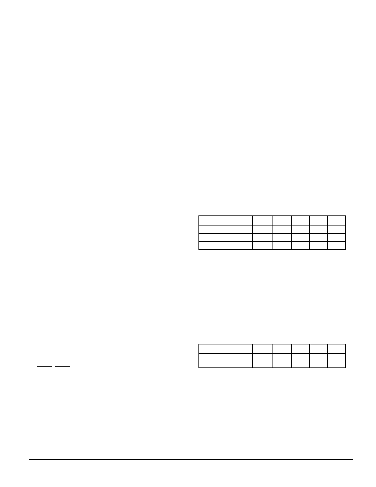
CONTROL PIN TIE VALUES (H ≥ VIH, L ≤ VIL)
5 V Device Numbers ADSP ADSC ADV SE1 LBO
MCM67C518
—
—
—
L
H
MCM67J518
—
—
—
—
H
MCM67N518
—
—
—
L
L
NOTE: If no tie value is given, then the pin should be used as intended
on the 5 V device.
NON–BURST SYNCHRONOUS OPERATION
Although this BurstRAM has been designed for PowerPC–
and Pentium – based systems, these SRAMs can be used in
other high speed L2 cache or memory applications that do not
require the burst address feature. Most L2 caches designed
with a synchronous interface can make use of the
MCM63P531. The burst counter feature of the
BurstRAM can be disabled, and the SRAM can be configured
to act upon a continuous stream of addresses. See Figure 2.
CONTROL PIN TIE VALUES (H ≥ VIH, L ≤ VIL)
Non–Burst
ADSP ADSC ADV SE1 LBO
Sync Non–Burst,
Pipelined SRAM
H
L
H
L
X
NOTE: Although X is specified in the table as a don’t care, the pin must
be tied either high or low.
MOTOROLA FAST SRAM
MCM63P531
11
Share Link: 