CY62256 데이터 시트보기 (PDF) - Cypress Semiconductor
부품명
상세내역
제조사
CY62256 Datasheet PDF : 12 Pages
| |||
CY62256
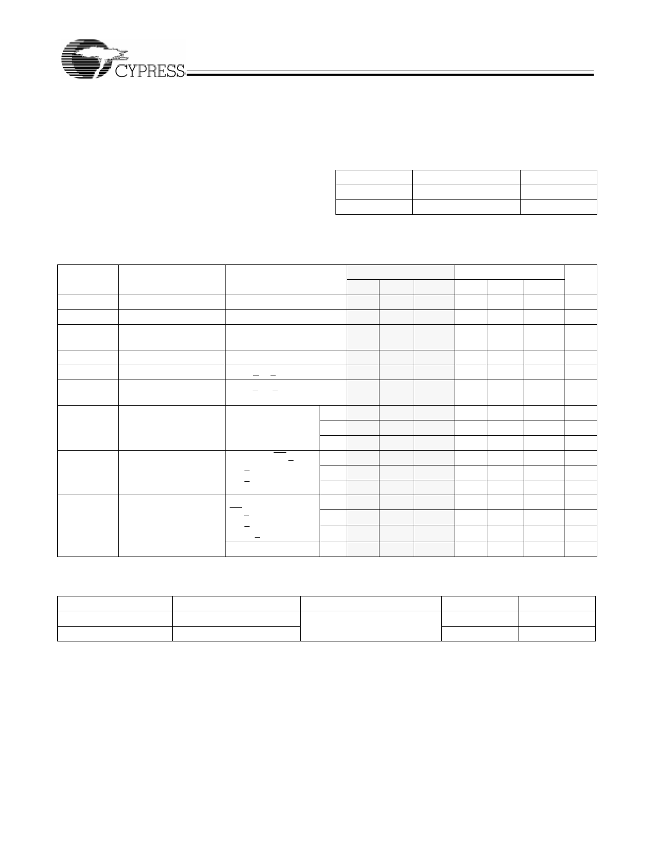
Maximum Ratings
(Above which the useful life may be impaired. For user guide-
lines, not tested.)
Storage Temperature ..................................... −65°C to +150°C
Ambient Temperature with
Power Applied ................................................... 0°C to +70°C
Supply Voltage to Ground Potential
(Pin 28 to Pin 14).................................................−0.5V to +7.0V
DC Voltage Applied to Outputs
in High Z State[1] ....................................... −0.5V to VCC + 0.5V
DC Input Voltage[1].................................... −0.5V to VCC + 0.5V
Output Current into Outputs (LOW)............................. 20 mA
Static Discharge Voltage .......................................... >2001V
(per MIL-STD-883, Method 3015)
Latch-Up Current.................................................... >200 mA
Operating Range
Range
Commercial
Industrial
Ambient Temperature
0°C to +70°C
–40°C to +85°C
VCC
5V ± 10%
5V ± 10%
Electrical Characteristics Over the Operating Range
Parameter
VOH
VOL
VIH
Description
Output HIGH Voltage
Output LOW Voltage
Input HIGH Voltage
VIL
Input LOW Voltage
IIX
Input Load Current
IOZ
Output Leakage
Current
ICC
VCC Operating Supply
Current
ISB1
Automatic CE
Power-Down Current—
TTL Inputs
ISB2
Automatic CE
Power-Down Current—
CMOS Inputs
Shaded area contains preliminary information.
Test Conditions
VCC = Min., IOH = −1.0 mA
VCC = Min., IOL = 2.1 mA
GND < VI < VCC
GND < VO < VCC, Output Dis-
abled
VCC = Max.,
IOUT = 0 mA,
L
f = fMAX = 1/tRC
LL
Max. VCC, CE > VIH,
VIN > VIH or
L
VIN < VIL, f = fMAX
LL
Max. VCC,
CE > VCC − 0.3V
VIN > VCC − 0.3V
or VIN < 0.3V, f = 0
L
LL
Indust’l Temp Range LL
CY62256−55
Min. Typ[2] Max.
2.4
0.4
2.2
VCC
+0.5V
−0.5
0.8
−0.5
+0.5
−0.5
+0.5
28
55
25
50
25
50
0.5
2
0.4 0.6
0.3 0.5
1
5
2
50
0.1
5
0.1
10
CY62256−70
Min. Typ[2] Max.
2.4
0.4
2.2
VCC
+0.5V
−0.5
0.8
−0.5
+0.5
−0.5
+0.5
28
55
25
50
25
50
0.5
2
0.4
0.6
0.3
0.5
1
5
2
50
0.1
5
0.1
10
Unit
V
V
V
V
µA
µA
mA
mA
mA
mA
mA
mA
mA
µA
µA
µA
Capacitance[3]
Parameter
Description
Test Conditions
Max.
Unit
CIN
COUT
Input Capacitance
Output Capacitance
TA = 25°C, f = 1 MHz,
VCC = 5.0V
6
pF
8
pF
Note:
1. VIL (min.) = −2.0V for pulse durations of less than 20 ns.
2. Typical specifications are the mean values measured over a large sample size across normal production process variations and are taken at nominal conditions
(TA = 25°C, VCC). Parameters are guaranteed by design and characterization, and not 100% tested.
3. Tested initially and after any design or process changes that may affect these parameters.
2
Share Link: 