NT7501H-BDT 데이터 시트보기 (PDF) - Novatek Microelectronics
부품명
상세내역
제조사
NT7501H-BDT Datasheet PDF : 38 Pages
| |||
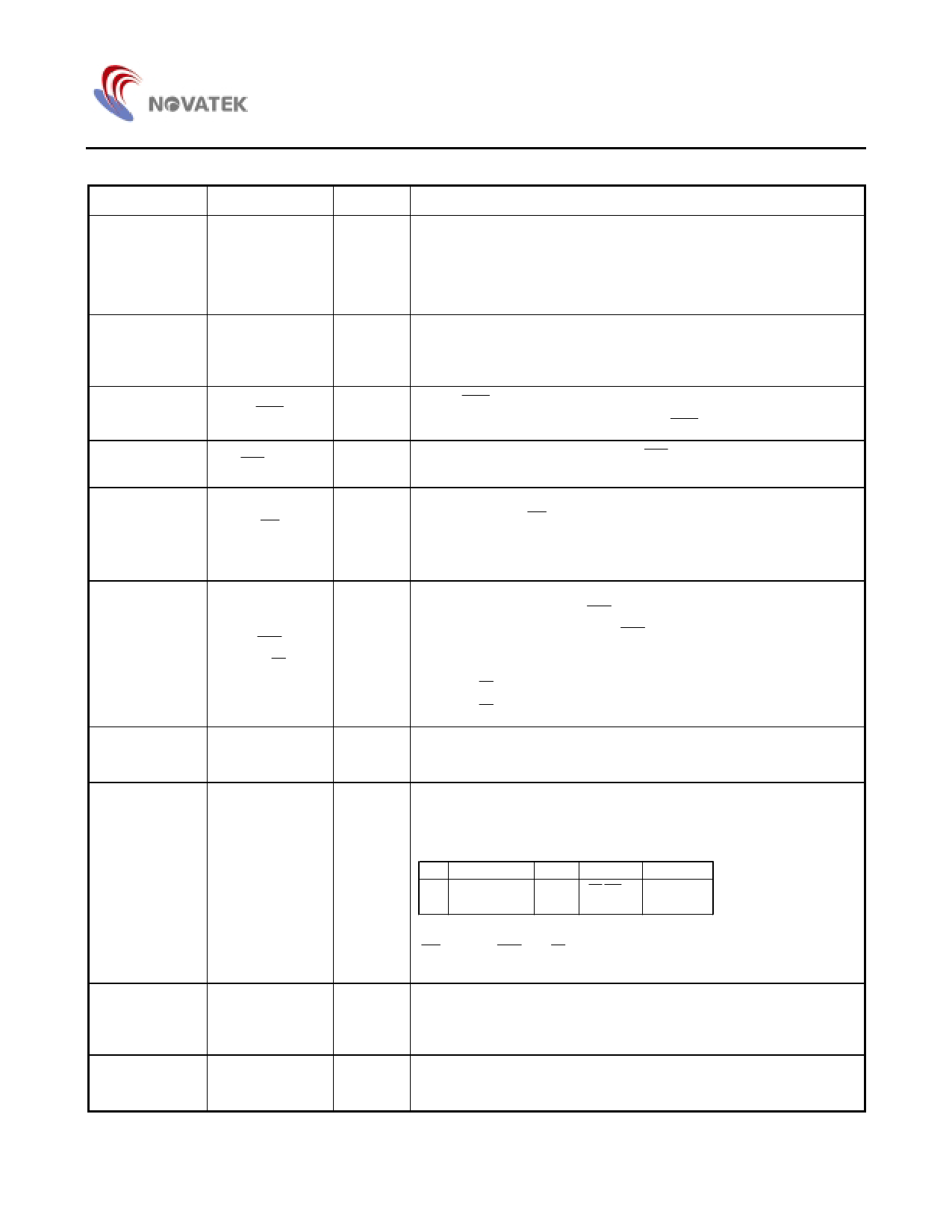
System Bus Connection Terminals
Pad No.
Symbol
27 - 34
D0 - D7
(SI)
(SCL)
16
8
11 - 13
18
A0
RES
CS1 CS2
RD
(E)
17
WR
(RW )
14
C86
10
P/S
7
M/S
4
CL
NT7501
I/O
Description
This is an 8-bit bi-directional data bus that connects to an 8-bit or 16-bit
standard MPU data bus.
I/O
When the serial interface is selected (P/S = “L”), then D7 serves as the
serial data input terminal (SI) and D6 serves as the serial clock input
terminal (SCL). At this time, D0 to D5 are set to high impedance.
When the chip select is inactive, D0 to D7 are set to high impedance.
This is connected to the least significant bit of the normal MPU address
I
bus, and it determines whether the data bits are data or a command.
A0 = “H”: Indicate that D0 to D7 are display data.
A0 = “L”: Indicates that D0 to D7 are control data.
When RES is set to “L”, the settings are initialized.
I
The reset operation is performed by the RES signal level.
I
This is the chip select signal. When CS1 = “L” and CS2 = “H”, then the
chip select becomes active and data/command I/O are enabled
When connected to an 8080 MPU, it is active LOW. This pad is
connected to the RD signal of the 8080MPU, and the NT7501 data bus
I
is in an output statue when this signal is “L”.
When connected to a 6800 Series MPU, this is active HIGH. This is
used as an enable clock input of the 6800 series MPU.
When connected to an 8080 MPU, this is active LOW. This terminal
connects to the 8080 MPU WR signal . The signals on the data bus are
latched at the rising edge of the WR signal.
I
When connected to a 6800 Series MPU: This is the read/write control
signal input terminal.
When R W = “H”: Read.
When R W = “L”: Write.
This is the MPU interface switch terminal.
I
C86 = “H”: 6800 Series MPU interface.
C86 = “L”: 8080 Series MPU interface.
This is the parallel data input/serial data input switch terminal.
P/S = “H”: Parallel data input.
P/S = “L”: Serial data input.
The following applies depending on the P/S status:
P/S Data/Command Data Read/Write Serial Clock
I
"H"
A0
D0 to D7 RD WR
"L"
A0
SI (D7) Write only SCL (D6)
When P/S = “L”, D0 to D5 are HZ. D0 to D5 may be “H”, “L” or Open.
RD (E) and WR ( R / W ) are fixed to either “H” or “L”. With serial data
input, RAM display data reading is not supported.
This terminal selects the master/slave operation for the NT7501 chips.
I
Master operation outputs the timing signals that are required for the
LCD display, while slave operation inputs the timing signals required for
the liquid crystal display, synchronizing the liquid crystal display system.
This is the display clock input terminal. When the NT7501 chips are
I/O
used in master/slave mode, the various CL terminals must be
connected.
5
Share Link: 