NT7501 데이터 시트보기 (PDF) - Novatek Microelectronics
부품명
상세내역
제조사
NT7501 Datasheet PDF : 38 Pages
| |||
NT7501
Busy Flag
The Busy flag is set when the NT7501 starts to operate. During operation, it accepts Read Status instruction only. The busy flag
signal is output at pad D7 when Read Status is issued. If the cycle time (tCYC) is correct, the microprocessor need not check the
flag before issuing a command. This can greatly improve the microprocessor performance.
Initial Display Line Register
When the display RAM data is read, the display line, according to COM0 (usually, the top line of screen), is determined using
register data. The register is also used for screen scrolling and page switching.
The set Display Start Line command sets the 6-bit display start address in this register. The register data is preset on the line
counter each time the FR signal status changes. The line counter is incremented by CL signal and it generates a line address to
allow 132 bit.
Column Address Counter
This is a 8 bit presettable counter that provides the column address to the display RAM (refer to Figure4). It is incremented by 1
when a Read/Write command is entered. However, the counter is not incremented but locked if a non-existing address above
84H is specified. It is unlocked when a column address is set again. The Column Address counter is independent of the Page
Address register.
When the ADC Select command is issued to display an inverse display, the column address decoder inverts the relationship
between the RAM column address and the display segment output.
Page Address Register
This is a 4-bit page address register that provides a page address to the display RAM (refer to Figure 4). The microprocessor
issues Set Page Address command to change the page and access to another page. Page address 8 (D3 is high, but D2,D1
and D0 are low) is RAM area dedicated to the indicator, and only display data D0 is valid.
Display Data RAM
The display data RAM stores pixel data for the LCD. It is a 65-column by 132-row (8-page by 8 bit + 1) addressable array. Each
pixel can be selected when the page and column addresses are specified.
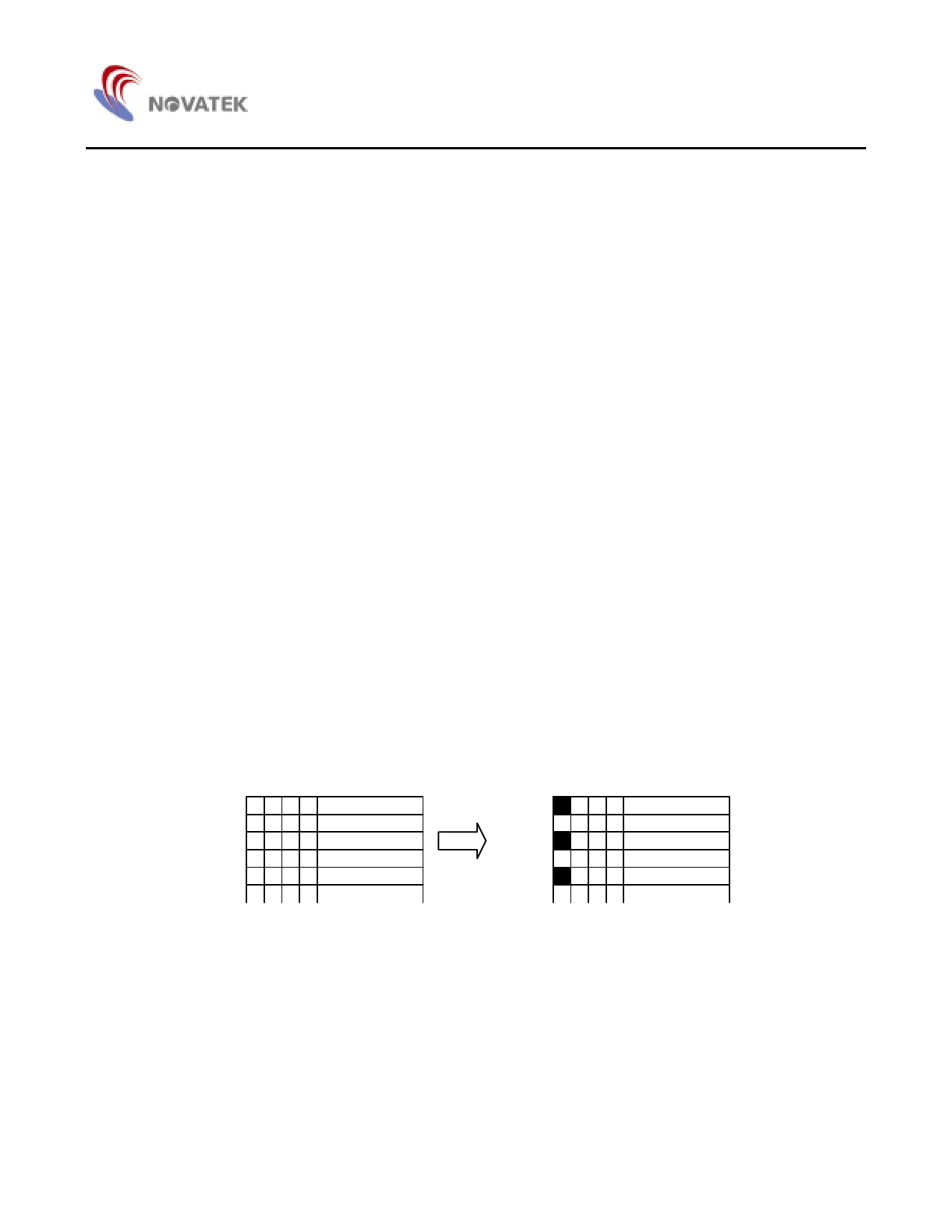
The time required to transfer data is very short because the microprocessor enters D0 to D7 corresponding to the LCD common
lines as shown in Figure 3. Therefore, multiple NT7501’s can easily configure a large display having high flexibility with very
little data transmission restriction.
The microprocessor writes and reads data to/from the RAM through the I/O buffer. As the LCD controller operates
independently, data can be written into the RAM at the same time as the data is being displayed, without causing the LCD to
flicker.
D0 1
D1 0
D2 1
D3 0
D4 1
COM0
COM1
COM2
COM3
COM4
Display data RAM
Figure 3.
Display on LCD
9
Share Link: 