DG211CJZ 데이터 시트보기 (PDF) - Intersil
부품명
상세내역
제조사
DG211CJZ Datasheet PDF : 7 Pages
| |||
DG211
Electrical Specifications
PARAMETER
V+ = +15V, V- = -15V, VL = +5V, GND, TA = 25°C (Continued)
TEST CONDITIONS
(NOTE 4) (NOTE 5)
MIN
TYP
MAX
UNITS
POWER SUPPLY CHARACTERISTICS
Positive Supply Current, I+
Negative Supply Current, I-
VIN = 0V or 2.4V
-
0.1
10
µA
-
0.1
10
µA
Logic Supply Current, IL
-
0.1
10
µA
NOTES:
4. The algebraic convention whereby the most negative value is a minimum, and the most positive is a maximum, is used in this data sheet.
5. For design reference only, not 100% tested.
6. ID(ON) is leakage from driver into ON switch.
7.
OFF Isolation
=
20
log
-V----S--
VD
,
VS
=
Input to OFF switch, VD
=
output .
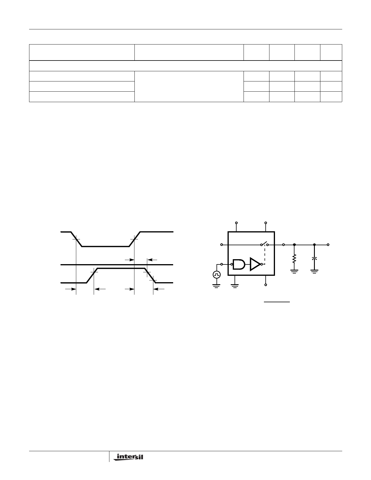
Test Circuits and Waveforms
Switch output waveform shown for VS = constant with logic
input waveform as shown. Note the VS may be + or - as per
switching time test circuit. VO is the steady state output with
switch on. Feedthrough via gate capacitance may result in
spikes at leading and trailing edge of output waveform.
LOGIC†
INPUT (IN1)
tr < 20ns
tf < 20ns
SWITCH
INPUT
VS
SWITCH
OUTPUT (VO)
50%
0V
90%
tON
tOFF1
90%
10%
tOFF2
† Logic shown for DG211.
FIGURE 1. SWITCHING TIME MEASUREMENT POINTS
SWITCH
INPUT S1
VS = 10V
5V
VL
LOGIC IN1
INPUT
15V
V+
SWITCH
D1
OUTPUT
VO
RL
CL
1kΩ
35pF
GND
V-
-15V
(REPEAT TEST FOR
IN2, IN3 AND IN4)
RL
VO = VS RL + rDS(ON)
FIGURE 2. SWITCHING TIME TEST CIRCUIT
4
FN3118.4
December 21, 2005
Share Link: 