DG2714 데이터 시트보기 (PDF) - Vishay Semiconductors
부품명
상세내역
제조사
DG2714 Datasheet PDF : 8 Pages
| |||
DG2714
Vishay Siliconix
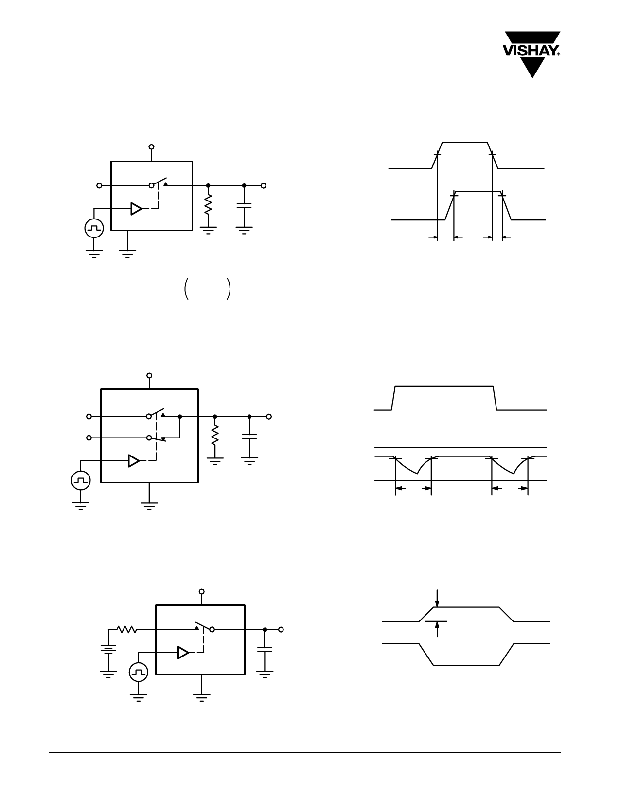
TEST CIRCUITS
Switch
Input
Logic
Input
V+
V+
NO or NC
COM
IN
GND
Switch Output
VOUT
RL
300 Ω
CL
35 pF
CL (includes fixture and stray capacitance)
VOUT =
VCOM
RL
RL + RON
Logic
Input
Switch
Output
VINH
VINL
50 %
tr < 5 ns
tf < 5 ns
0.9 x VOUT
0V
tON
tOFF
Logic "1" = Switch On
Logic input waveforms inverted for switches that have
the opposite logic sense.
Figure 1. Switching Time
V+
V+
NO
VNO
COM
NC
VNC
IN
GND
RL
300 Ω
Logic
Input
VO
VINH
VINL
CL
35 pF
VNC = VNO
VO
Switch
0V
Output
90 %
tD
CL (includes fixture and stray capacitance)
Figure 2. Break-Before-Make Interval
tr < 5 ns
tf < 5 ns
tD
V+
Vgen
Rgen
+
VIN = 0 - V+
COM
V+
NC or NO
IN
GND
www.vishay.com
6
VOUT
VOUT
ΔVOUT
CL = 1 nF
IN
On
Off
On
Q = ΔVOUT x CL
IN depends on switch configuration: input polarity
determined by sense of switch.
Figure 3. Charge Injection
Document Number: 72308
S-70852-Rev. B, 30-Apr-07
Share Link: 